

Intel UHD Graphics 620 vs NVIDIA GeForce MX150
Intel UHD Graphics 620
► remove from comparison
The Intel UHD Graphics 620 (GT2) is an integrated graphics unit, which can be found in various ULV (Ultra Low Voltage) processors of the Kaby Lake Refresh generation (8th generation Core). Compared to the similar named Intel HD Graphics 620 in the 2016 Kaby Lake CPUs, only the name changed from HD to UHD. It is clocked with up to 1.150 MHz and therefore 100 MHz higher than the old HD Graphics 620 (max. 1.050 MHz) and offer a comparable performance. Due to its lack of dedicated graphics memory or eDRAM cache, the HD 620 has to access the main memory (2x 64bit DDR3/DDR4).
Performance
The exact performance of the UHD Graphics 620 depends on various factors like L3 cache size, memory configuration (DDR3/DDR4) and maximum clock rate of the specific model and as is similar to the Intel HD Graphics 620 and Intel HD Graphics 630. Compared to the average HD Graphics 620, the UHD graphics profits from the quad-core CPU a bit in our gaming benchmarks. Therefore, should be positioned between a GeForce 910M and 920M dedicated graphics card from Nvidia. For games, the drivers however are not that fast updated and tested as with GeForce graphics cards. In our tests, the UHD 620 is most suited for casual games like Team Fortress 2, Rocket League or Farming Simulator 17. See below for a list of modern games tested with various models.
Features
The revised video engine now supports H.265/HEVC Main10 profile in hardware with 10 bit colors. Furthermore, Googles VP9 codec can also be hardware decoded. The first models do not support HDCP 2.2 and therefore Netflix 4K. This was added with the new models in 2017 and beginning of May 2017 also the older CPU models like the i3-7100U are now shipped with a new S-Spec Code that supports HDCP 2.2. HDMI 2.0 however is still only supported with an external converter chip (LSPCon).
Power Consumption
The UHD Graphics 620 can be found in mobile processors specified at 15 W TDP and is therefore suited for compact laptops and ultrabooks. The power consumption during playing The Witcher 3 (with an external monitor) was comparable to a Intel HD Graphics 620 based laptop and on the lowest end of all of our measurements. Dedicated GPUs, like the GeForce 940MX, needed a lot more power.
NVIDIA GeForce MX150
► remove from comparison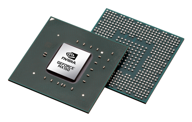
The Nvidia GeForce MX150 is a dedicated entry-level mobile graphics card for laptops based on the GP108 chip with the Pascal architecture. It was announced mid 2017 and is the mobile version of the desktop GeForce GT 1030. It offers the same 384 shader cores and 64 Bit memory bus manufactured in 14 nm. The clock rates and performance however are a bit higher than the desktop GT 1030. Officially it is the successor to the older Maxwell based GeForce 940MX.
Currently there are two variants of the MX150, a "normal" N17S-G1-A1 with 1468 - 1531 MHz and 25 Watt TDP and a power efficient variant named N17S-LG-A1 with 936 - 1037 MHz (-32%) and 10 Watt TDP (-60%) for thin and light laptops.
The GP108 chip is manufactured in a 14 nm FinFET process at Samsung (LPP) and offers a number of new features, including support for DisplayPort 1.4 (ready), HDMI 2.0b, HDR and improved H.265 video de- and encoding (PlayReady 3.0). 4K HDR with Netflix however wont run due to the minimum 3 GB graphics memory that is required. Compared to the bigger Pascal chips, the small GP108 does not support Simultaneous Multi-Projection (SMP) for VR and G-Sync. A full list of improvements and the new Pascal desktop GPUs is available in our dedicated Pascal architecture article.
The performance however is higher than the old GeForce GTX 950M with GDDR5 memory. Still modern and demanding games only run in low settings and resolutions fluently. E.g. Assassin's Creed Origins was only playable in lowest settings and 1280x720 pixels. Less demanding games like Call of Duty WW2 also ran in medium settings and Full HD fluently. See below for more and detailed gaming benchmarks.
The power efficient N17S-LG-A1 ULV variant is clearly slower than the normal one (due to the 32% lower boost clock).
The power consumption (25 Watt TDP of the chip alone) however lies on a level of the old 940MX (23 Watt). The older 950M and the new GTX 1050 are rated much higher with 40 Watt TDP. The GeForce MX150 also uses a small 23 x 23 mm package due to the small chip size.
| Intel UHD Graphics 620 | NVIDIA GeForce MX150 | |||||||||||||||||||||||||||||||||||||||||||||||||
| GeForce MX100 Series |
|
| ||||||||||||||||||||||||||||||||||||||||||||||||
| Codename | Kaby-Lake-Refresh GT2 | N17S-G1 | ||||||||||||||||||||||||||||||||||||||||||||||||
| Architecture | Gen. 9.5 | Pascal | ||||||||||||||||||||||||||||||||||||||||||||||||
| Pipelines | 24 - unified | 384 - unified | ||||||||||||||||||||||||||||||||||||||||||||||||
| Core Speed | 300 - 1150 (Boost) MHz | 1468 - 1532 (Boost) MHz | ||||||||||||||||||||||||||||||||||||||||||||||||
| Theoretical Performance | 883 TFLOPS FP16, 442 TFLOPS FP32, 110.4 TFLOPS FP64 | |||||||||||||||||||||||||||||||||||||||||||||||||
| Memory Type | DDR3/DDR4 | GDDR5 | ||||||||||||||||||||||||||||||||||||||||||||||||
| Shared Memory | yes | no | ||||||||||||||||||||||||||||||||||||||||||||||||
| API | DirectX 12_1, OpenGL 4.4 | DirectX 12_1, OpenGL 4.5 | ||||||||||||||||||||||||||||||||||||||||||||||||
| technology | 14 nm | 14 nm | ||||||||||||||||||||||||||||||||||||||||||||||||
| Displays | HDMI 1.4, DisplayPort 1.2 | |||||||||||||||||||||||||||||||||||||||||||||||||
| Features | QuickSync | Vulkan, Multi Monitor, Nvidia Optimus | ||||||||||||||||||||||||||||||||||||||||||||||||
| Date of Announcement | 01.09.2017 | 16.05.2017 | ||||||||||||||||||||||||||||||||||||||||||||||||
| Predecessor | HD Graphics 620 | GeForce 940MX | ||||||||||||||||||||||||||||||||||||||||||||||||
| TMUs | 24 | |||||||||||||||||||||||||||||||||||||||||||||||||
| ROPs | 16 | |||||||||||||||||||||||||||||||||||||||||||||||||
| Memory Speed | 6008 effective = 1502 MHz | |||||||||||||||||||||||||||||||||||||||||||||||||
| Memory Bus Width | 64 Bit | |||||||||||||||||||||||||||||||||||||||||||||||||
| Max. Amount of Memory | 4 GB | |||||||||||||||||||||||||||||||||||||||||||||||||
| Memory Bandwidth | 40.1 GB/s | |||||||||||||||||||||||||||||||||||||||||||||||||
| Power Consumption | 25 Watt (10 - 25 Watt TGP) | |||||||||||||||||||||||||||||||||||||||||||||||||
| Transistors | 1.8 Billion | |||||||||||||||||||||||||||||||||||||||||||||||||
| Die Size | 71 mm² | |||||||||||||||||||||||||||||||||||||||||||||||||
| PCIe | 3 x4 | |||||||||||||||||||||||||||||||||||||||||||||||||
| Link to Manufacturer Page | www.geforce.com | |||||||||||||||||||||||||||||||||||||||||||||||||
| Successor | GeForce MX250 |
| |||||||||||||||||||||||||||||||||||||||||||||||||||||||||||||||||||||||||||||||||||||
Benchmarks
| Model | CPU | GPU | RAM | Value |
|---|---|---|---|---|
| Dell Latitude 15 3510 NK2MC | i3-10110U 51 W / 22 W | UHD Graphics 620 1000 MHz | 8 GB | 2133 |
| Prime Computer PrimeMini 5 i7 NUC8v7PNB | i7-8665U 16 W / 16 W | UHD Graphics 620 | 16 GB | 2773 |
| Dynabook Satellite Pro C50-E-105 | i5-8250U 25 W / 15 W | UHD Graphics 620 1100 MHz | 8 GB | 2916 |
Schenker Office 15  | i5-10210U 15 W / 15 W | UHD Graphics 620 1100 MHz | 16 GB | 3091 |
| Dell Latitude 12 7210 2-in-1 | i7-10610U 51 W / 23 W | UHD Graphics 620 1150 MHz | 16 GB | 3306 |
| Model | CPU | GPU | RAM | Value |
|---|---|---|---|---|
| Acer Chromebook Spin 713 CP713-2W-560V | i5-10210U | UHD Graphics 620 1100 MHz | 8 GB | 7727 |
| Model | CPU | GPU | RAM | Value |
|---|---|---|---|---|
| Acer Chromebook Spin 713 CP713-2W-560V | i5-10210U | UHD Graphics 620 1100 MHz | 8 GB | 8007 |
| Model | CPU | GPU | RAM | Value |
|---|---|---|---|---|
| Acer Chromebook Spin 713 CP713-2W-560V | i5-10210U | UHD Graphics 620 1100 MHz | 8 GB | 5204 |
| Lenovo IdeaPad Flex 5 CB 13IML05 82B80010GE | i5-10210U | UHD Graphics 620 1100 MHz | 8 GB | 5549 |
| Model | CPU | GPU | RAM | Value |
|---|---|---|---|---|
| Acer Chromebook Spin 713 CP713-2W-560V | i5-10210U | UHD Graphics 620 1100 MHz | 8 GB | 4856 |
| Lenovo IdeaPad Flex 5 CB 13IML05 82B80010GE | i5-10210U | UHD Graphics 620 1100 MHz | 8 GB | 5190 |
| Model | CPU | GPU | RAM | Value |
|---|---|---|---|---|
| Dell Latitude 7410 Chromebook Enterprise | i5-10310U | UHD Graphics 620 450 MHz 1 GB | 16 GB | 4525 |
| Dell Latitude 7410 Chromebook Enterprise 2-in-1 | i5-10310U | UHD Graphics 620 ? / 1150 MHz 1 GB | 16 GB | 5493 |
| Acer Chromebook Spin 713 CP713-2W-560V | i5-10210U | UHD Graphics 620 1100 MHz | 8 GB | 5821 |
| Acer Chromebook 715 CB715-1WT-527F | i5-8350U | UHD Graphics 620 | 8 GB | 6103 |
| Model | CPU | GPU | RAM | Value |
|---|---|---|---|---|
| Dell Latitude 7410 Chromebook Enterprise | i5-10310U | UHD Graphics 620 450 MHz 1 GB | 16 GB | 4362 |
| Acer Chromebook Spin 713 CP713-2W-560V | i5-10210U | UHD Graphics 620 1100 MHz | 8 GB | 5948 |
| Dell Latitude 7410 Chromebook Enterprise 2-in-1 | i5-10310U | UHD Graphics 620 ? / 1150 MHz 1 GB | 16 GB | 6156 |
| Acer Chromebook 715 CB715-1WT-527F | i5-8350U | UHD Graphics 620 | 8 GB | 7204 |
| Model | CPU | GPU | RAM | Value |
|---|---|---|---|---|
| Acer Chromebook Spin 713 CP713-2W-560V | i5-10210U | UHD Graphics 620 1100 MHz | 8 GB | 4254 |
| Lenovo IdeaPad Flex 5 CB 13IML05 82B80010GE | i5-10210U | UHD Graphics 620 1100 MHz | 8 GB | 4529 |
| Acer Chromebook 715 CB715-1WT-527F | i5-8350U | UHD Graphics 620 | 8 GB | 4538 |
| Model | CPU | GPU | RAM | Value |
|---|---|---|---|---|
| Acer Chromebook Spin 713 CP713-2W-560V | i5-10210U | UHD Graphics 620 1100 MHz | 8 GB | 3992 |
| Lenovo IdeaPad Flex 5 CB 13IML05 82B80010GE | i5-10210U | UHD Graphics 620 1100 MHz | 8 GB | 4248 |
| Acer Chromebook 715 CB715-1WT-527F | i5-8350U | UHD Graphics 620 | 8 GB | 4735 |
3DM Vant. Perf. total + Intel UHD Graphics 620
| Model | CPU | GPU | RAM | Value |
|---|---|---|---|---|
| Minipc Union NiPoGi CK10 - 10810U | i7-10810U 40 W / 15 W | UHD Graphics 620 1150 / 1333 MHz | 16 GB | 6899 |
| Asus ZenBook 14 UX433FA | i7-8565U | UHD Graphics 620 | 16 GB | 7761 |
| Model | CPU | GPU | RAM | Value |
|---|---|---|---|---|
| Lenovo ThinkPad T480s-20L8S02E00 | i5-8550U | GeForce MX150 1038 / 1252.5 MHz 2 GB | 16 GB | 7839 |
| Acer Aspire 5 A515-51G-51RL | i5-7200U | GeForce MX150 1683 / 1502 MHz 2 GB | 8 GB | 14144 |
| Model | CPU | GPU | RAM | Value |
|---|---|---|---|---|
| Minipc Union NiPoGi CK10 - 10810U | i7-10810U 40 W / 15 W | UHD Graphics 620 1150 / 1333 MHz | 16 GB | 5555 |
| Asus ZenBook 14 UX433FA | i7-8565U | UHD Graphics 620 | 16 GB | 6341 |
| Model | CPU | GPU | RAM | Value |
|---|---|---|---|---|
| Lenovo ThinkPad T480s-20L8S02E00 | i5-8550U | GeForce MX150 1038 / 1252.5 MHz 2 GB | 16 GB | 6377 |
| Acer Aspire 5 A515-51G-51RL | i5-7200U | GeForce MX150 1683 / 1502 MHz 2 GB | 8 GB | 15132 |
| Model | CPU | GPU | RAM | Value |
|---|---|---|---|---|
| Honor Magicbook | i5-8250U | UHD Graphics 620 1468 / 6008 MHz | 8 GB | 34467 |
| Model | CPU | GPU | RAM | Value |
|---|---|---|---|---|
| Honor Magicbook | i5-8250U | GeForce MX150 1468 / 6008 MHz 2 GB | 8 GB | 34443 |
| Model | CPU | GPU | RAM | Value |
|---|---|---|---|---|
| Minipc Union NiPoGi CK10 - 10810U | i7-10810U 40 W / 15 W | UHD Graphics 620 1150 / 1333 MHz | 16 GB | 16972 |
| Model | CPU | GPU | RAM | Value | |
|---|---|---|---|---|---|
| 3DMark 06 - Standard 1280x1024 | |||||
| Acer Swift 3 SF314-55-31N8 (3DMark 06 - Standard 1280x1024) | i3-8145U | UHD Graphics 620 1000 MHz | 4 GB | 7653 | |
| Acer Aspire 3 A315-51-30YA (3DMark 06 - Standard 1280x1024) | i3-8130U | UHD Graphics 620 1000 MHz | 4.1 GB | 7844 | |
| Lenovo ThinkPad X380 Yoga 20LJS02W00 (3DMark 06 - Standard 1280x1024) | i5-8550U | UHD Graphics 620 1150 MHz | 16 GB | 8282 | |
| Acer Extensa 15 EX215-51-56UX (3DMark 06 - Standard 1280x1024) | i5-10210U | UHD Graphics 620 1100 MHz | 8 GB | 9074 | |
| Dell Latitude 7390 2-in-1 (3DMark 06 - Standard 1280x1024) | i7-8650U | UHD Graphics 620 1150 / 1067 MHz | 16 GB | 9648 | |
| Fujitsu Lifebook U938 (3DMark 06 - Standard 1280x1024) | i5-8250U | UHD Graphics 620 1100 MHz | 12 GB | 9851 | |
| Lenovo V330-15IKB (3DMark 06 - Standard 1280x1024) | i3-7130U | UHD Graphics 620 1000 MHz | 8 GB | 9886 | |
| Lenovo ThinkPad E490-20N8000RGE (3DMark 06 - Standard 1280x1024) | i5-8265U | UHD Graphics 620 1100 MHz | 8 GB | 10006 | |
| Dell Latitude 13 5300 2-in-1 (3DMark 06 - Standard 1280x1024) | i5-8365U | UHD Graphics 620 300 / 1200 MHz | 8 GB | 10108 | |
| Lenovo ThinkPad X380 Yoga-20LH000LUS (3DMark 06 - Standard 1280x1024) | i5-8250U | UHD Graphics 620 400 / 1197 MHz 1 GB | 7.9 GB | 10245 | |
| HP Spectre x360 13-ae048ng (3DMark 06 - Standard 1280x1024) | i5-8550U | UHD Graphics 620 400 / 1064 MHz | 16 GB | 10323 | |
| Dell Inspiron 14 5000 5482 2-in-1 (3DMark 06 - Standard 1280x1024) | i7-8565U | UHD Graphics 620 300 / 1200 MHz | 8 GB | 10342 | |
| HP Pavilion x360 14-dh1153ng (3DMark 06 - Standard 1280x1024) | i5-10210U | UHD Graphics 620 1100 MHz | 8 GB | 10342 | |
| Dell Latitude 7390 (3DMark 06 - Standard 1280x1024) | i7-8650U | UHD Graphics 620 1150 MHz | 8 GB | 10376 | |
| Dell Latitude 5290 2-in-1 (3DMark 06 - Standard 1280x1024) | i5-8350U | UHD Graphics 620 1100 MHz | 8 GB | 10387 | |
| HP Spectre x360 13t-ae000 (3DMark 06 - Standard 1280x1024) | i5-8550U | UHD Graphics 620 1150 / 1067 MHz | 16 GB | 10406 | |
| HP Elite x2 1013 G3-2TT14EA (3DMark 06 - Standard 1280x1024) | i5-8350U | UHD Graphics 620 1100 MHz | 8 GB | 10622 | |
| Acer Spin 5 SP513-52N-566U (3DMark 06 - Standard 1280x1024) | i5-8250U | UHD Graphics 620 | 8 GB | 10662 | |
| Asus ZenBook Flip 14 UX461UA (3DMark 06 - Standard 1280x1024) | i5-8250U | UHD Graphics 620 1100 MHz | 8 GB | 10737 | |
| Dell Latitude 7400 2-in-1 (3DMark 06 - Standard 1280x1024) | i7-8665U | UHD Graphics 620 1150 MHz | 16 GB | 10985 | |
| Dell Latitude 7400-8N6DH (3DMark 06 - Standard 1280x1024) | i7-8665U | UHD Graphics 620 1150 / 1200 MHz | 16 GB | 11053 | |
| Asus ZenBook 14 UX433FA (3DMark 06 - Standard 1280x1024) | i7-8565U | UHD Graphics 620 | 16 GB | 11207 | |
| Asus Zenbook 14 UX433FA-A6018T (3DMark 06 - Standard 1280x1024) | i5-8265U | UHD Graphics 620 1100 MHz | 8 GB | 11338 | |
| Minipc Union NiPoGi CK10 - 10810U (3DMark 06 - Standard 1280x1024) | i7-10810U 40 W / 15 W | UHD Graphics 620 1150 / 1333 MHz | 16 GB | 11379 | |
| LG Gram 15Z980-B.AA78B (3DMark 06 - Standard 1280x1024) | i5-8550U | UHD Graphics 620 | 16 GB | 11397 | |
| Lenovo IdeaPad 730S-13IWL 81JB0004US (3DMark 06 - Standard 1280x1024) | i5-8265U | UHD Graphics 620 1100 MHz | 8 GB | 11535 | |
| Dell Latitude 5490 (3DMark 06 - Standard 1280x1024) | i7-8650U | UHD Graphics 620 1150 MHz | 8 GB | 11732 | |
| Lenovo V320-17IKB-81CN000MGE (3DMark 06 - Standard 1280x1024) | i5-8250U | UHD Graphics 620 1100 MHz | 8 GB | 11950 | |
| Tuxedo InfinityBook Pro 13 2017 (3DMark 06 - Standard 1280x1024) | i5-8550U | UHD Graphics 620 | 32 GB | 12051 | |
| Acer Swift 5 SF515-51T-76B6 (3DMark 06 - Standard 1280x1024) | i7-8565U | UHD Graphics 620 1150 MHz | 16 GB | 12132 | |
| Lenovo ThinkPad X1 Yoga 2018-20LD0015US (3DMark 06 - Standard 1280x1024) | i5-8250U | UHD Graphics 620 400 / 1064 MHz 1 GB | 7.9 GB | 12344 | |
| Dell Latitude 9510 2-in-1 (3DMark 06 - Standard 1280x1024) | i7-10810U | UHD Graphics 620 300 / 1064 MHz | 16 GB | 12453 | |
| Dell Latitude 7410 (3DMark 06 - Standard 1280x1024) | i7-10610U | UHD Graphics 620 300 / 1330 MHz | 16 GB | 13918 | |
| Dell XPS 13 7390 Core i7-10710U (3DMark 06 - Standard 1280x1024) | i7-10710U | UHD Graphics 620 | 16 GB | 14158 | |
| Model | CPU | GPU | RAM | Value | |
|---|---|---|---|---|---|
| 3DMark 06 - Standard 1280x1024 | |||||
| Lenovo ThinkPad T480s-20L8S02E00 (3DMark 06 - Standard 1280x1024) | i5-8550U | GeForce MX150 1038 / 1252.5 MHz 2 GB | 16 GB | 12796 | |
| Asus ZenBook 13 UX331UN (3DMark 06 - Standard 1280x1024) | i5-8550U | GeForce MX150 1607 / 1253 MHz 2 GB | 8 GB | 12911 | |
| HP Envy 13-ah0003ng (3DMark 06 - Standard 1280x1024) | i5-8550U | GeForce MX150 1038 / 1253 MHz 2 GB | 16 GB | 17106 | |
| Acer Aspire 5 A517-51G-80L (3DMark 06 - Standard 1280x1024) | i5-8550U | GeForce MX150 1532 / 6000 MHz 2 GB | 8 GB | 17583 | |
| Asus Zenbook 14 UX433FN-A6023T (3DMark 06 - Standard 1280x1024) | i7-8565U | GeForce MX150 1038 / 1253 MHz 2 GB | 16 GB | 19038 | |
| Xiaomi Mi Notebook Air 13.3 2018 (3DMark 06 - Standard 1280x1024) | i5-8250U | GeForce MX150 936 / 1250 MHz 2 GB | 8 GB | 19210 | |
| Acer Aspire 5 A515-51G-51RL (3DMark 06 - Standard 1280x1024) | i5-7200U | GeForce MX150 1683 / 1502 MHz 2 GB | 8 GB | 19415 | |
| Clevo N855H1 (3DMark 06 - Standard 1280x1024) | i3-7100H | GeForce MX150 1532 / 1502 MHz 2 GB | 8 GB | 20343 | |
| Acer Swift 3 SF315-51G-57E5 (3DMark 06 - Standard 1280x1024) | i5-8250U | GeForce MX150 1798 / 1502 MHz 2 GB | 8 GB | 22407 | |
| Dell Inspiron 17-7786 (3DMark 06 - Standard 1280x1024) | i7-8565U | GeForce MX150 1532 / 6000 MHz 2 GB | 16 GB | 22583 | |
| Acer Aspire 5 A515-52G-53PU (3DMark 06 - Standard 1280x1024) | i5-8265U | GeForce MX150 1532 / 1502 MHz 2 GB | 8 GB | 22890 | |
| MSI PL62 MX150 7700HQ (3DMark 06 - Standard 1280x1024) | i7-7700HQ | GeForce MX150 | 16 GB | 24726 | |
| Model | CPU | GPU | RAM | Value |
|---|---|---|---|---|
| Minipc Union NiPoGi CK10 - 10810U | i7-10810U 40 W / 15 W | UHD Graphics 620 1150 / 1333 MHz | 16 GB | 3.9 |
| Acer Spin 5 SP513-52N-566U | i5-8250U | UHD Graphics 620 | 8 GB | 4.7 |
| LG Gram 15Z980-B.AA78B | i5-8550U | UHD Graphics 620 | 16 GB | 5.5 |
| Model | CPU | GPU | RAM | Value |
|---|---|---|---|---|
| Xiaomi Mi Notebook Air 13.3 2018 | i5-8250U | GeForce MX150 936 / 1250 MHz 2 GB | 8 GB | 14.6 |
| Acer Aspire 5 A515-51G-51RL | i5-7200U | GeForce MX150 1683 / 1502 MHz 2 GB | 8 GB | 16.8 |
| Model | CPU | GPU | RAM | Value |
|---|---|---|---|---|
| Honor Magicbook | i5-8250U | UHD Graphics 620 1468 / 6008 MHz | 8 GB | 19.2 |
| Model | CPU | GPU | RAM | Value |
|---|---|---|---|---|
| Acer Aspire 5 A515-51G-51RL | i5-7200U | GeForce MX150 1683 / 1502 MHz 2 GB | 8 GB | 41.8 |
| Model | CPU | GPU | RAM | Value |
|---|---|---|---|---|
| Lenovo ThinkPad T480s-20L8S02E00 | i5-8550U | GeForce MX150 1038 / 1252.5 MHz 2 GB | 16 GB | 27 |
| Acer Aspire 5 A515-51G-51RL | i5-7200U | GeForce MX150 1683 / 1502 MHz 2 GB | 8 GB | 56.9 |
specvp12 sw-03 + Intel UHD Graphics 620
| Model | CPU | GPU | RAM | Value |
|---|---|---|---|---|
| Dell Latitude 13 3390 | i5-8250U | UHD Graphics 620 | 8 GB | 17.99 |
| Lenovo ThinkPad L390 Yoga-20NT000XGE | i5-8265U | UHD Graphics 620 1100 / 1200 MHz | 8 GB | 21.93 |
| Intel NUC10i5FNK | i5-10210U | UHD Graphics 620 | 8 GB | 23.86 |
| Acer Swift 3 SF313-51-59SZ | i5-8250U | UHD Graphics 620 1100 / 1200 MHz | 8 GB | 24.09 |
| HP ProBook 440 G6-5TK01EA | i7-8565U | UHD Graphics 620 | 16 GB | 24.55 |
| Lenovo ThinkBook 15 | i5-10210U | UHD Graphics 620 | 16 GB | 26.13 |
| Intel NUC10i7FNH | i7-10710U | UHD Graphics 620 | 16 GB | 28.71 |
| Model | CPU | GPU | RAM | Value |
|---|---|---|---|---|
| Acer Aspire 5 A515-51G-51RL | i5-7200U | GeForce MX150 1683 / 1502 MHz 2 GB | 8 GB | 23.01 |
| Xiaomi Mi Notebook Air 13.3 2018 | i5-8250U | GeForce MX150 936 / 1250 MHz 2 GB | 8 GB | 24.42 |
| Dell Inspiron 17-7786 | i7-8565U | GeForce MX150 1532 / 6000 MHz 2 GB | 16 GB | 24.99 |
| Model | CPU | GPU | RAM | Value |
|---|---|---|---|---|
| Lenovo ThinkPad L390 Yoga-20NT000XGE | i5-8265U | UHD Graphics 620 1100 / 1200 MHz | 8 GB | 2.49 |
| Dell Latitude 13 3390 | i5-8250U | UHD Graphics 620 | 8 GB | 2.56 |
| Lenovo ThinkBook 15 | i5-10210U | UHD Graphics 620 | 16 GB | 2.58 |
| Intel NUC10i5FNK | i5-10210U | UHD Graphics 620 | 8 GB | 2.67 |
| HP ProBook 440 G6-5TK01EA | i7-8565U | UHD Graphics 620 | 16 GB | 2.68 |
| Acer Swift 3 SF313-51-59SZ | i5-8250U | UHD Graphics 620 1100 / 1200 MHz | 8 GB | 2.73 |
| Intel NUC10i7FNH | i7-10710U | UHD Graphics 620 | 16 GB | 2.98 |
| Model | CPU | GPU | RAM | Value |
|---|---|---|---|---|
| Acer Aspire 5 A515-51G-51RL | i5-7200U | GeForce MX150 1683 / 1502 MHz 2 GB | 8 GB | 3.07 |
| Xiaomi Mi Notebook Air 13.3 2018 | i5-8250U | GeForce MX150 936 / 1250 MHz 2 GB | 8 GB | 3.08 |
| Dell Inspiron 17-7786 | i7-8565U | GeForce MX150 1532 / 6000 MHz 2 GB | 16 GB | 3.26 |
| Model | CPU | GPU | RAM | Value |
|---|---|---|---|---|
| Lenovo ThinkPad L390 Yoga-20NT000XGE | i5-8265U | UHD Graphics 620 1100 / 1200 MHz | 8 GB | 5 |
| HP ProBook 440 G6-5TK01EA | i7-8565U | UHD Graphics 620 | 16 GB | 5.53 |
| Acer Swift 3 SF313-51-59SZ | i5-8250U | UHD Graphics 620 1100 / 1200 MHz | 8 GB | 6.61 |
| Intel NUC10i5FNK | i5-10210U | UHD Graphics 620 | 8 GB | 6.81 |
| Dell Latitude 13 3390 | i5-8250U | UHD Graphics 620 | 8 GB | 6.9 |
| Lenovo ThinkBook 15 | i5-10210U | UHD Graphics 620 | 16 GB | 8.03 |
| Intel NUC10i7FNH | i7-10710U | UHD Graphics 620 | 16 GB | 8.35 |
| Model | CPU | GPU | RAM | Value |
|---|---|---|---|---|
| Xiaomi Mi Notebook Air 13.3 2018 | i5-8250U | GeForce MX150 936 / 1250 MHz 2 GB | 8 GB | 13.22 |
| Acer Aspire 5 A515-51G-51RL | i5-7200U | GeForce MX150 1683 / 1502 MHz 2 GB | 8 GB | 13.93 |
| Dell Inspiron 17-7786 | i7-8565U | GeForce MX150 1532 / 6000 MHz 2 GB | 16 GB | 15.8 |
| Model | CPU | GPU | RAM | Value |
|---|---|---|---|---|
| Intel NUC10i5FNK | i5-10210U | UHD Graphics 620 | 8 GB | 2.62 |
| Lenovo ThinkBook 15 | i5-10210U | UHD Graphics 620 | 16 GB | 2.68 |
| HP ProBook 440 G6-5TK01EA | i7-8565U | UHD Graphics 620 | 16 GB | 2.8 |
| Intel NUC10i7FNH | i7-10710U | UHD Graphics 620 | 16 GB | 2.91 |
| Lenovo ThinkPad L390 Yoga-20NT000XGE | i5-8265U | UHD Graphics 620 1100 / 1200 MHz | 8 GB | 3.09 |
| Acer Swift 3 SF313-51-59SZ | i5-8250U | UHD Graphics 620 1100 / 1200 MHz | 8 GB | 3.49 |
| Dell Latitude 13 3390 | i5-8250U | UHD Graphics 620 | 8 GB | 9.17 |
| Model | CPU | GPU | RAM | Value |
|---|---|---|---|---|
| Dell Inspiron 17-7786 | i7-8565U | GeForce MX150 1532 / 6000 MHz 2 GB | 16 GB | 9.81 |
| Xiaomi Mi Notebook Air 13.3 2018 | i5-8250U | GeForce MX150 936 / 1250 MHz 2 GB | 8 GB | 10.28 |
| Acer Aspire 5 A515-51G-51RL | i5-7200U | GeForce MX150 1683 / 1502 MHz 2 GB | 8 GB | 11.55 |
| Model | CPU | GPU | RAM | Value |
|---|---|---|---|---|
| Dell Latitude 13 3390 | i5-8250U | UHD Graphics 620 | 8 GB | 4.27 |
| Lenovo ThinkPad L390 Yoga-20NT000XGE | i5-8265U | UHD Graphics 620 1100 / 1200 MHz | 8 GB | 11.34 |
| HP ProBook 440 G6-5TK01EA | i7-8565U | UHD Graphics 620 | 16 GB | 11.58 |
| Intel NUC10i5FNK | i5-10210U | UHD Graphics 620 | 8 GB | 13.02 |
| Acer Swift 3 SF313-51-59SZ | i5-8250U | UHD Graphics 620 1100 / 1200 MHz | 8 GB | 13.1 |
| Lenovo ThinkBook 15 | i5-10210U | UHD Graphics 620 | 16 GB | 13.87 |
| Intel NUC10i7FNH | i7-10710U | UHD Graphics 620 | 16 GB | 15.71 |
| Model | CPU | GPU | RAM | Value |
|---|---|---|---|---|
| Acer Aspire 5 A515-51G-51RL | i5-7200U | GeForce MX150 1683 / 1502 MHz 2 GB | 8 GB | 25.1 |
| Xiaomi Mi Notebook Air 13.3 2018 | i5-8250U | GeForce MX150 936 / 1250 MHz 2 GB | 8 GB | 26.24 |
| Dell Inspiron 17-7786 | i7-8565U | GeForce MX150 1532 / 6000 MHz 2 GB | 16 GB | 32.06 |
| Model | CPU | GPU | RAM | Value |
|---|---|---|---|---|
| Acer Swift 3 SF313-51-59SZ | i5-8250U | UHD Graphics 620 1100 / 1200 MHz | 8 GB | 0.22 |
| HP ProBook 440 G6-5TK01EA | i7-8565U | UHD Graphics 620 | 16 GB | 0.22 |
| Lenovo ThinkBook 15 | i5-10210U | UHD Graphics 620 | 16 GB | 0.23 |
| Intel NUC10i5FNK | i5-10210U | UHD Graphics 620 | 8 GB | 0.23 |
| Lenovo ThinkPad L390 Yoga-20NT000XGE | i5-8265U | UHD Graphics 620 1100 / 1200 MHz | 8 GB | 0.24 |
| Intel NUC10i7FNH | i7-10710U | UHD Graphics 620 | 16 GB | 0.28 |
| Dell Latitude 13 3390 | i5-8250U | UHD Graphics 620 | 8 GB | 0.81 |
| Model | CPU | GPU | RAM | Value |
|---|---|---|---|---|
| Xiaomi Mi Notebook Air 13.3 2018 | i5-8250U | GeForce MX150 936 / 1250 MHz 2 GB | 8 GB | 0.49 |
| Dell Inspiron 17-7786 | i7-8565U | GeForce MX150 1532 / 6000 MHz 2 GB | 16 GB | 0.49 |
| Acer Aspire 5 A515-51G-51RL | i5-7200U | GeForce MX150 1683 / 1502 MHz 2 GB | 8 GB | 0.56 |
| Model | CPU | GPU | RAM | Value |
|---|---|---|---|---|
| Dell Latitude 13 3390 | i5-8250U | UHD Graphics 620 | 8 GB | 7.9 |
| Acer Swift 3 SF313-51-59SZ | i5-8250U | UHD Graphics 620 1100 / 1200 MHz | 8 GB | 12.37 |
| Lenovo ThinkPad L390 Yoga-20NT000XGE | i5-8265U | UHD Graphics 620 1100 / 1200 MHz | 8 GB | 12.51 |
| HP ProBook 440 G6-5TK01EA | i7-8565U | UHD Graphics 620 | 16 GB | 12.85 |
| Intel NUC10i5FNK | i5-10210U | UHD Graphics 620 | 8 GB | 12.93 |
| Lenovo ThinkBook 15 | i5-10210U | UHD Graphics 620 | 16 GB | 13.66 |
| Intel NUC10i7FNH | i7-10710U | UHD Graphics 620 | 16 GB | 14.42 |
| Model | CPU | GPU | RAM | Value |
|---|---|---|---|---|
| Acer Aspire 5 A515-51G-51RL | i5-7200U | GeForce MX150 1683 / 1502 MHz 2 GB | 8 GB | 11.08 |
| Xiaomi Mi Notebook Air 13.3 2018 | i5-8250U | GeForce MX150 936 / 1250 MHz 2 GB | 8 GB | 11.17 |
| Dell Inspiron 17-7786 | i7-8565U | GeForce MX150 1532 / 6000 MHz 2 GB | 16 GB | 11.52 |
| Model | CPU | GPU | RAM | Value |
|---|---|---|---|---|
| Dell Latitude 13 3390 | i5-8250U | UHD Graphics 620 | 8 GB | 7.38 |
| Lenovo ThinkPad L390 Yoga-20NT000XGE | i5-8265U | UHD Graphics 620 1100 / 1200 MHz | 8 GB | 12.55 |
| HP ProBook 440 G6-5TK01EA | i7-8565U | UHD Graphics 620 | 16 GB | 13.05 |
| Acer Swift 3 SF313-51-59SZ | i5-8250U | UHD Graphics 620 1100 / 1200 MHz | 8 GB | 13.79 |
| Intel NUC10i5FNK | i5-10210U | UHD Graphics 620 | 8 GB | 14.12 |
| Lenovo ThinkBook 15 | i5-10210U | UHD Graphics 620 | 16 GB | 15.73 |
| Intel NUC10i7FNH | i7-10710U | UHD Graphics 620 | 16 GB | 16.55 |
| Model | CPU | GPU | RAM | Value |
|---|---|---|---|---|
| Xiaomi Mi Notebook Air 13.3 2018 | i5-8250U | GeForce MX150 936 / 1250 MHz 2 GB | 8 GB | 16.44 |
| Acer Aspire 5 A515-51G-51RL | i5-7200U | GeForce MX150 1683 / 1502 MHz 2 GB | 8 GB | 16.86 |
| Dell Inspiron 17-7786 | i7-8565U | GeForce MX150 1532 / 6000 MHz 2 GB | 16 GB | 17.85 |
| Model | CPU | GPU | RAM | Value |
|---|---|---|---|---|
| Lenovo ThinkPad L390 Yoga-20NT000XGE | i5-8265U | UHD Graphics 620 1100 / 1200 MHz | 8 GB | 10.98 |
| HP ProBook 440 G6-5TK01EA | i7-8565U | UHD Graphics 620 | 16 GB | 12.25 |
| Intel NUC10i5FNK | i5-10210U | UHD Graphics 620 | 8 GB | 12.92 |
| Acer Swift 3 SF313-51-59SZ | i5-8250U | UHD Graphics 620 1100 / 1200 MHz | 8 GB | 12.95 |
| Dell Latitude 13 3390 | i5-8250U | UHD Graphics 620 | 8 GB | 13.48 |
| Lenovo ThinkBook 15 | i5-10210U | UHD Graphics 620 | 16 GB | 14.45 |
| Intel NUC10i7FNH | i7-10710U | UHD Graphics 620 | 16 GB | 15.22 |
| Model | CPU | GPU | RAM | Value |
|---|---|---|---|---|
| Xiaomi Mi Notebook Air 13.3 2018 | i5-8250U | GeForce MX150 936 / 1250 MHz 2 GB | 8 GB | 22.02 |
| Dell Inspiron 17-7786 | i7-8565U | GeForce MX150 1532 / 6000 MHz 2 GB | 16 GB | 23.92 |
| Model | CPU | GPU | RAM | Value |
|---|---|---|---|---|
| Lenovo ThinkPad L390 Yoga-20NT000XGE | i5-8265U | UHD Graphics 620 1100 / 1200 MHz | 8 GB | 27.99 |
| Intel NUC10i5FNK | i5-10210U | UHD Graphics 620 | 8 GB | 31.48 |
| HP ProBook 440 G6-5TK01EA | i7-8565U | UHD Graphics 620 | 16 GB | 31.69 |
| Acer Swift 3 SF313-51-59SZ | i5-8250U | UHD Graphics 620 1100 / 1200 MHz | 8 GB | 31.86 |
| Dell Latitude 13 3390 | i5-8250U | UHD Graphics 620 | 8 GB | 32.14 |
| Lenovo ThinkBook 15 | i5-10210U | UHD Graphics 620 | 16 GB | 33.89 |
| Intel NUC10i7FNH | i7-10710U | UHD Graphics 620 | 16 GB | 37.6 |
| Model | CPU | GPU | RAM | Value |
|---|---|---|---|---|
| Dell Inspiron 17-7786 | i7-8565U | GeForce MX150 1532 / 6000 MHz 2 GB | 16 GB | 35.28 |
| Model | CPU | GPU | RAM | Value |
|---|---|---|---|---|
| Lenovo ThinkPad L390 Yoga-20NT000XGE | i5-8265U | UHD Graphics 620 1100 / 1200 MHz | 8 GB | 4.37 |
| Lenovo ThinkBook 15 | i5-10210U | UHD Graphics 620 | 16 GB | 4.64 |
| Intel NUC10i5FNK | i5-10210U | UHD Graphics 620 | 8 GB | 4.8 |
| HP ProBook 440 G6-5TK01EA | i7-8565U | UHD Graphics 620 | 16 GB | 4.87 |
| Acer Swift 3 SF313-51-59SZ | i5-8250U | UHD Graphics 620 1100 / 1200 MHz | 8 GB | 4.89 |
| Dell Latitude 13 3390 | i5-8250U | UHD Graphics 620 | 8 GB | 5.28 |
| Intel NUC10i7FNH | i7-10710U | UHD Graphics 620 | 16 GB | 5.37 |
| Model | CPU | GPU | RAM | Value |
|---|---|---|---|---|
| Dell Inspiron 17-7786 | i7-8565U | GeForce MX150 1532 / 6000 MHz 2 GB | 16 GB | 5.87 |
| Model | CPU | GPU | RAM | Value |
|---|---|---|---|---|
| Lenovo ThinkPad L390 Yoga-20NT000XGE | i5-8265U | UHD Graphics 620 1100 / 1200 MHz | 8 GB | 4.99 |
| HP ProBook 440 G6-5TK01EA | i7-8565U | UHD Graphics 620 | 16 GB | 5.49 |
| Acer Swift 3 SF313-51-59SZ | i5-8250U | UHD Graphics 620 1100 / 1200 MHz | 8 GB | 6.68 |
| Intel NUC10i5FNK | i5-10210U | UHD Graphics 620 | 8 GB | 6.81 |
| Dell Latitude 13 3390 | i5-8250U | UHD Graphics 620 | 8 GB | 6.87 |
| Lenovo ThinkBook 15 | i5-10210U | UHD Graphics 620 | 16 GB | 8 |
| Intel NUC10i7FNH | i7-10710U | UHD Graphics 620 | 16 GB | 8.34 |
| Model | CPU | GPU | RAM | Value |
|---|---|---|---|---|
| Dell Inspiron 17-7786 | i7-8565U | GeForce MX150 1532 / 6000 MHz 2 GB | 16 GB | 15.73 |
| Model | CPU | GPU | RAM | Value |
|---|---|---|---|---|
| Dell Latitude 13 3390 | i5-8250U | UHD Graphics 620 | 8 GB | 1.96 |
| Acer Swift 3 SF313-51-59SZ | i5-8250U | UHD Graphics 620 1100 / 1200 MHz | 8 GB | 2.09 |
| Intel NUC10i5FNK | i5-10210U | UHD Graphics 620 | 8 GB | 2.12 |
| Lenovo ThinkPad L390 Yoga-20NT000XGE | i5-8265U | UHD Graphics 620 1100 / 1200 MHz | 8 GB | 2.15 |
| Lenovo ThinkBook 15 | i5-10210U | UHD Graphics 620 | 16 GB | 2.18 |
| Intel NUC10i7FNH | i7-10710U | UHD Graphics 620 | 16 GB | 2.23 |
| HP ProBook 440 G6-5TK01EA | i7-8565U | UHD Graphics 620 | 16 GB | 2.26 |
| Model | CPU | GPU | RAM | Value |
|---|---|---|---|---|
| Dell Inspiron 17-7786 | i7-8565U | GeForce MX150 1532 / 6000 MHz 2 GB | 16 GB | 8.46 |
| Model | CPU | GPU | RAM | Value |
|---|---|---|---|---|
| Lenovo ThinkPad L390 Yoga-20NT000XGE | i5-8265U | UHD Graphics 620 1100 / 1200 MHz | 8 GB | 15.66 |
| HP ProBook 440 G6-5TK01EA | i7-8565U | UHD Graphics 620 | 16 GB | 17.55 |
| Intel NUC10i5FNK | i5-10210U | UHD Graphics 620 | 8 GB | 18.97 |
| Acer Swift 3 SF313-51-59SZ | i5-8250U | UHD Graphics 620 1100 / 1200 MHz | 8 GB | 19.58 |
| Dell Latitude 13 3390 | i5-8250U | UHD Graphics 620 | 8 GB | 19.99 |
| Lenovo ThinkBook 15 | i5-10210U | UHD Graphics 620 | 16 GB | 21.36 |
| Intel NUC10i7FNH | i7-10710U | UHD Graphics 620 | 16 GB | 22.97 |
| Model | CPU | GPU | RAM | Value |
|---|---|---|---|---|
| Dell Inspiron 17-7786 | i7-8565U | GeForce MX150 1532 / 6000 MHz 2 GB | 16 GB | 54.2 |
| Model | CPU | GPU | RAM | Value |
|---|---|---|---|---|
| Lenovo ThinkPad L390 Yoga-20NT000XGE | i5-8265U | UHD Graphics 620 1100 / 1200 MHz | 8 GB | 0.21 |
| Lenovo ThinkBook 15 | i5-10210U | UHD Graphics 620 | 16 GB | 0.68 |
| Intel NUC10i7FNH | i7-10710U | UHD Graphics 620 | 16 GB | 0.73 |
| Intel NUC10i5FNK | i5-10210U | UHD Graphics 620 | 8 GB | 1.42 |
| Acer Swift 3 SF313-51-59SZ | i5-8250U | UHD Graphics 620 1100 / 1200 MHz | 8 GB | 1.79 |
| Dell Latitude 13 3390 | i5-8250U | UHD Graphics 620 | 8 GB | 2.85 |
| Model | CPU | GPU | RAM | Value |
|---|---|---|---|---|
| Lenovo ThinkPad L390 Yoga-20NT000XGE | i5-8265U | UHD Graphics 620 1100 / 1200 MHz | 8 GB | 15.15 |
| Intel NUC10i5FNK | i5-10210U | UHD Graphics 620 | 8 GB | 16.77 |
| Acer Swift 3 SF313-51-59SZ | i5-8250U | UHD Graphics 620 1100 / 1200 MHz | 8 GB | 16.93 |
| HP ProBook 440 G6-5TK01EA | i7-8565U | UHD Graphics 620 | 16 GB | 16.97 |
| Dell Latitude 13 3390 | i5-8250U | UHD Graphics 620 | 8 GB | 17.12 |
| Lenovo ThinkBook 15 | i5-10210U | UHD Graphics 620 | 16 GB | 18.11 |
| Intel NUC10i7FNH | i7-10710U | UHD Graphics 620 | 16 GB | 18.88 |
| Model | CPU | GPU | RAM | Value |
|---|---|---|---|---|
| Dell Inspiron 17-7786 | i7-8565U | GeForce MX150 1532 / 6000 MHz 2 GB | 16 GB | 27.12 |
| Model | CPU | GPU | RAM | Value |
|---|---|---|---|---|
| Lenovo ThinkPad L390 Yoga-20NT000XGE | i5-8265U | UHD Graphics 620 1100 / 1200 MHz | 8 GB | 17.43 |
| HP ProBook 440 G6-5TK01EA | i7-8565U | UHD Graphics 620 | 16 GB | 18.42 |
| Dell Latitude 13 3390 | i5-8250U | UHD Graphics 620 | 8 GB | 19.63 |
| Intel NUC10i5FNK | i5-10210U | UHD Graphics 620 | 8 GB | 19.97 |
| Acer Swift 3 SF313-51-59SZ | i5-8250U | UHD Graphics 620 1100 / 1200 MHz | 8 GB | 20.3 |
| Lenovo ThinkBook 15 | i5-10210U | UHD Graphics 620 | 16 GB | 22.4 |
| Intel NUC10i7FNH | i7-10710U | UHD Graphics 620 | 16 GB | 23.37 |
| Model | CPU | GPU | RAM | Value |
|---|---|---|---|---|
| Dell Inspiron 17-7786 | i7-8565U | GeForce MX150 1532 / 6000 MHz 2 GB | 16 GB | 25.75 |
| Model | CPU | GPU | RAM | Value |
|---|---|---|---|---|
| Lenovo ThinkPad L390 Yoga-20NT000XGE | i5-8265U | UHD Graphics 620 1100 / 1200 MHz | 8 GB | 10.82 |
| HP ProBook 440 G6-5TK01EA | i7-8565U | UHD Graphics 620 | 16 GB | 12.14 |
| Intel NUC10i5FNK | i5-10210U | UHD Graphics 620 | 8 GB | 12.71 |
| Dell Latitude 13 3390 | i5-8250U | UHD Graphics 620 | 8 GB | 13.08 |
| Acer Swift 3 SF313-51-59SZ | i5-8250U | UHD Graphics 620 1100 / 1200 MHz | 8 GB | 13.38 |
| Lenovo ThinkBook 15 | i5-10210U | UHD Graphics 620 | 16 GB | 14.29 |
| Intel NUC10i7FNH | i7-10710U | UHD Graphics 620 | 16 GB | 15.01 |
| Model | CPU | GPU | RAM | Value |
|---|---|---|---|---|
| Dell Inspiron 17-7786 | i7-8565U | GeForce MX150 1532 / 6000 MHz 2 GB | 16 GB | 23.25 |
Cinebench R15 OpenGL 64 Bit + Intel UHD Graphics 620
| Model | CPU | GPU | RAM | Value |
|---|---|---|---|---|
| HP Chromebook x360 14 G1 | i5-8350U | UHD Graphics 620 1100 MHz | 8 GB | 9.9 |
| Dell Latitude 7410 Chromebook Enterprise | i5-10310U | UHD Graphics 620 450 MHz 1 GB | 16 GB | 10 |
| Dell Latitude 7410 Chromebook Enterprise 2-in-1 | i5-10310U | UHD Graphics 620 ? / 1150 MHz 1 GB | 16 GB | 16 |
| Model | CPU | GPU | RAM | Value |
|---|---|---|---|---|
| HP Chromebook x360 14 G1 | i5-8350U | UHD Graphics 620 1100 MHz | 8 GB | 26 |
| Dell Latitude 7410 Chromebook Enterprise | i5-10310U | UHD Graphics 620 450 MHz 1 GB | 16 GB | 27 |
| Dell Latitude 7410 Chromebook Enterprise 2-in-1 | i5-10310U | UHD Graphics 620 ? / 1150 MHz 1 GB | 16 GB | 27 |
| Model | CPU | GPU | RAM | Value |
|---|---|---|---|---|
| HP Chromebook x360 14 G1 | i5-8350U | UHD Graphics 620 1100 MHz | 8 GB | 24 |
| Dell Latitude 7410 Chromebook Enterprise | i5-10310U | UHD Graphics 620 450 MHz 1 GB | 16 GB | 24 |
| Dell Latitude 7410 Chromebook Enterprise 2-in-1 | i5-10310U | UHD Graphics 620 ? / 1150 MHz 1 GB | 16 GB | 25 |
| Tuxedo InfinityBook Pro 14 | i7-8565U | UHD Graphics 620 1150 MHz | 32 GB | 27.5 |
| Acer Spin 5 SP513-52N-566U | i5-8250U | UHD Graphics 620 | 8 GB | 30.5 |
| Asus ZenBook 14 UX433FA | i7-8565U | UHD Graphics 620 | 16 GB | 33.01 |
| Tuxedo InfinityBook Pro 14 Windows 10 | i7-8565U | UHD Graphics 620 1150 MHz | 32 GB | 34.4 |
| Model | CPU | GPU | RAM | Value |
|---|---|---|---|---|
| Asus ZenBook 13 UX331UN | i5-8550U | GeForce MX150 1607 / 1253 MHz 2 GB | 8 GB | 52.9 |
| Lenovo ThinkPad T480s-20L8S02E00 | i5-8550U | GeForce MX150 1038 / 1252.5 MHz 2 GB | 16 GB | 61.6 |
| Xiaomi Mi Notebook Air 13.3 2018 | i5-8250U | GeForce MX150 936 / 1250 MHz 2 GB | 8 GB | 62 |
| Acer Aspire 5 A515-51G-51RL | i5-7200U | GeForce MX150 1683 / 1502 MHz 2 GB | 8 GB | 75.4 |
| Model | CPU | GPU | RAM | Value |
|---|---|---|---|---|
| Dell Latitude 7410 Chromebook Enterprise 2-in-1 | i5-10310U | UHD Graphics 620 ? / 1150 MHz 1 GB | 16 GB | 22 |
| Asus ZenBook 14 UX433FA | i7-8565U | UHD Graphics 620 | 16 GB | 29.69 |
| HP Chromebook x360 14 G1 | i5-8350U | UHD Graphics 620 1100 MHz | 8 GB | 38 |
| Tuxedo InfinityBook Pro 14 | i7-8565U | UHD Graphics 620 1150 MHz | 32 GB | 41.6 |
| Acer Spin 5 SP513-52N-566U | i5-8250U | UHD Graphics 620 | 8 GB | 42.6 |
| Tuxedo InfinityBook Pro 14 Windows 10 | i7-8565U | UHD Graphics 620 1150 MHz | 32 GB | 45.7 |
| Model | CPU | GPU | RAM | Value |
|---|---|---|---|---|
| Asus ZenBook 13 UX331UN | i5-8550U | GeForce MX150 1607 / 1253 MHz 2 GB | 8 GB | 85.1 |
| Lenovo ThinkPad T480s-20L8S02E00 | i5-8550U | GeForce MX150 1038 / 1252.5 MHz 2 GB | 16 GB | 89.7 |
| Xiaomi Mi Notebook Air 13.3 2018 | i5-8250U | GeForce MX150 936 / 1250 MHz 2 GB | 8 GB | 92.1 |
| Acer Aspire 5 A515-51G-51RL | i5-7200U | GeForce MX150 1683 / 1502 MHz 2 GB | 8 GB | 111.5 |
| Model | CPU | GPU | RAM | Value |
|---|---|---|---|---|
| Dell Latitude 7410 Chromebook Enterprise | i5-10310U | UHD Graphics 620 450 MHz 1 GB | 16 GB | 0 |
| Asus ZenBook 14 UX433FA | i7-8565U | UHD Graphics 620 | 16 GB | 38.5 |
| HP Chromebook x360 14 G1 | i5-8350U | UHD Graphics 620 1100 MHz | 8 GB | 56 |
| Tuxedo InfinityBook Pro 14 | i7-8565U | UHD Graphics 620 1150 MHz | 32 GB | 61.8 |
| Acer Spin 5 SP513-52N-566U | i5-8250U | UHD Graphics 620 | 8 GB | 65.5 |
| Tuxedo InfinityBook Pro 14 Windows 10 | i7-8565U | UHD Graphics 620 1150 MHz | 32 GB | 70.7 |
| Model | CPU | GPU | RAM | Value |
|---|---|---|---|---|
| Lenovo ThinkPad T480s-20L8S02E00 | i5-8550U | GeForce MX150 1038 / 1252.5 MHz 2 GB | 16 GB | 121.5 |
| Asus ZenBook 13 UX331UN | i5-8550U | GeForce MX150 1607 / 1253 MHz 2 GB | 8 GB | 122.7 |
| Xiaomi Mi Notebook Air 13.3 2018 | i5-8250U | GeForce MX150 936 / 1250 MHz 2 GB | 8 GB | 125 |
| Acer Aspire 5 A515-51G-51RL | i5-7200U | GeForce MX150 1683 / 1502 MHz 2 GB | 8 GB | 148.7 |
GFXBench T-Rex HD Offscreen C24Z16 + Intel UHD Graphics 620
| Model | CPU | GPU | RAM | Value |
|---|---|---|---|---|
| Asus ZenBook 14 UX433FA | i7-8565U | UHD Graphics 620 | 16 GB | 73.3 |
| HP Chromebook x360 14 G1 | i5-8350U | UHD Graphics 620 1100 MHz | 8 GB | 114 |
| Tuxedo InfinityBook Pro 14 | i7-8565U | UHD Graphics 620 1150 MHz | 32 GB | 119.1 |
| Tuxedo InfinityBook Pro 14 Windows 10 | i7-8565U | UHD Graphics 620 1150 MHz | 32 GB | 130.4 |
| Acer Spin 5 SP513-52N-566U | i5-8250U | UHD Graphics 620 | 8 GB | 135 |
| Model | CPU | GPU | RAM | Value |
|---|---|---|---|---|
| Asus ZenBook 13 UX331UN | i5-8550U | GeForce MX150 1607 / 1253 MHz 2 GB | 8 GB | 203 |
| Lenovo ThinkPad T480s-20L8S02E00 | i5-8550U | GeForce MX150 1038 / 1252.5 MHz 2 GB | 16 GB | 205.8 |
| Xiaomi Mi Notebook Air 13.3 2018 | i5-8250U | GeForce MX150 936 / 1250 MHz 2 GB | 8 GB | 210 |
| Acer Aspire 5 A515-51G-51RL | i5-7200U | GeForce MX150 1683 / 1502 MHz 2 GB | 8 GB | 283.9 |
| Model | CPU | GPU | RAM | Value |
|---|---|---|---|---|
| Honor Magicbook bc7 | i5-8250U | UHD Graphics 620 1468 / 6008 MHz | 8 GB | 51.6 |
| Model | CPU | GPU | RAM | Value |
|---|---|---|---|---|
| Honor Magicbook bc7 | i5-8250U | GeForce MX150 1468 / 6008 MHz 2 GB | 8 GB | 140 |
| Model | CPU | GPU | RAM | Value |
|---|---|---|---|---|
| Honor Magicbook bc7 | i5-8250U | UHD Graphics 620 1468 / 6008 MHz | 8 GB | 4.44 |
| Model | CPU | GPU | RAM | Value |
|---|---|---|---|---|
| Minipc Union NiPoGi CK10 - 10810U | i7-10810U 40 W / 15 W | UHD Graphics 620 1150 / 1333 MHz | 16 GB | 4989 |
| Model | CPU | GPU | RAM | Value |
|---|---|---|---|---|
| Minipc Union NiPoGi CK10 - 10810U | i7-10810U 40 W / 15 W | UHD Graphics 620 1150 / 1333 MHz | 16 GB | 5447 |
| Model | CPU | GPU | RAM | Value |
|---|---|---|---|---|
| MSI Cubi 5 10M | i3-10110U | UHD Graphics 620 | 4 GB | 109 |
| Dell Latitude 7390 | i7-8650U | UHD Graphics 620 1150 MHz | 8 GB | 219 |
| Minipc Union NiPoGi CK10 - 10810U | i7-10810U 40 W / 15 W | UHD Graphics 620 1150 / 1333 MHz | 16 GB | 265 |
| Dell Latitude 5290 2-in-1 | i5-8350U | UHD Graphics 620 1100 MHz | 8 GB | 266 |
| Acer Spin 5 SP513-52N-566U | i5-8250U | UHD Graphics 620 | 8 GB | 275 |
| Intel NUC10i5FNK | i5-10210U | UHD Graphics 620 | 8 GB | 291 |
| Intel NUC10i7FNH | i7-10710U | UHD Graphics 620 | 16 GB | 291 |
| Dell Latitude 5490 | i7-8650U | UHD Graphics 620 1150 MHz | 8 GB | 304 |
| HP Spectre x360 13t-ae000 | i5-8550U | UHD Graphics 620 1150 / 1067 MHz | 16 GB | 309 |
| Tuxedo InfinityBook Pro 13 2017 | i5-8550U | UHD Graphics 620 | 32 GB | 319 |
| Asus ZenBook 14 UX433FA | i7-8565U | UHD Graphics 620 | 16 GB | 323 |
| Dell Latitude 7390 2-in-1 | i7-8650U | UHD Graphics 620 1150 / 1067 MHz | 16 GB | 325 |
| Lenovo ThinkPad X390-20Q1S02M00 | i5-8265U | UHD Graphics 620 | 16 GB | 336 |
| Model | CPU | GPU | RAM | Value |
|---|---|---|---|---|
| Asus ZenBook 13 UX331UN | i5-8550U | GeForce MX150 1607 / 1253 MHz 2 GB | 8 GB | 415 |
| Lenovo ThinkPad T480s-20L8S02E00 | i5-8550U | GeForce MX150 1038 / 1252.5 MHz 2 GB | 16 GB | 423 |
| Xiaomi Mi Notebook Air 13.3 2018 | i5-8250U | GeForce MX150 936 / 1250 MHz 2 GB | 8 GB | 429 |
| Acer Aspire 5 A515-51G-51RL | i5-7200U | GeForce MX150 1683 / 1502 MHz 2 GB | 8 GB | 446 |
| MSI PL62 MX150 7700HQ MX150 only | i7-7700HQ | GeForce MX150 | 16 GB | 456 |
| MSI PL62 MX150 7700HQ including Intel GPU | i7-7700HQ | GeForce MX150 | 16 GB | 769 |
| Model | CPU | GPU | RAM | Value |
|---|---|---|---|---|
| MSI Cubi 5 10M | i3-10110U | UHD Graphics 620 | 4 GB | 266 |
| Dell Latitude 5290 2-in-1 | i5-8350U | UHD Graphics 620 1100 MHz | 8 GB | 587 |
| Minipc Union NiPoGi CK10 - 10810U | i7-10810U 40 W / 15 W | UHD Graphics 620 1150 / 1333 MHz | 16 GB | 605 |
| Acer Spin 5 SP513-52N-566U | i5-8250U | UHD Graphics 620 | 8 GB | 622 |
| Dell Latitude 7390 | i7-8650U | UHD Graphics 620 1150 MHz | 8 GB | 622 |
| HP Spectre x360 13t-ae000 | i5-8550U | UHD Graphics 620 1150 / 1067 MHz | 16 GB | 633 |
| Tuxedo InfinityBook Pro 13 2017 | i5-8550U | UHD Graphics 620 | 32 GB | 653 |
| Dell Latitude 7390 2-in-1 | i7-8650U | UHD Graphics 620 1150 / 1067 MHz | 16 GB | 670 |
| Dell Latitude 5490 | i7-8650U | UHD Graphics 620 1150 MHz | 8 GB | 698 |
| Intel NUC10i5FNK | i5-10210U | UHD Graphics 620 | 8 GB | 736 |
| Intel NUC10i7FNH | i7-10710U | UHD Graphics 620 | 16 GB | 736 |
| Lenovo ThinkPad X390-20Q1S02M00 | i5-8265U | UHD Graphics 620 | 16 GB | 751 |
| Asus ZenBook 14 UX433FA | i7-8565U | UHD Graphics 620 | 16 GB | 755 |
| Model | CPU | GPU | RAM | Value |
|---|---|---|---|---|
| Asus ZenBook 13 UX331UN | i5-8550U | GeForce MX150 1607 / 1253 MHz 2 GB | 8 GB | 734 |
| Lenovo ThinkPad T480s-20L8S02E00 | i5-8550U | GeForce MX150 1038 / 1252.5 MHz 2 GB | 16 GB | 736 |
| Xiaomi Mi Notebook Air 13.3 2018 | i5-8250U | GeForce MX150 936 / 1250 MHz 2 GB | 8 GB | 757 |
| Acer Aspire 5 A515-51G-51RL | i5-7200U | GeForce MX150 1683 / 1502 MHz 2 GB | 8 GB | 790 |
| MSI PL62 MX150 7700HQ MX150 only | i7-7700HQ | GeForce MX150 | 16 GB | 805 |
| MSI PL62 MX150 7700HQ including Intel GPU | i7-7700HQ | GeForce MX150 | 16 GB | 1451 |
| Model | CPU | GPU | RAM | Value |
|---|---|---|---|---|
| Huawei Matebook X Pro i5 | i5-8250U | GeForce MX150 936 / 5010 MHz 2 GB | 8 GB | 2256 |
| Lenovo ThinkPad T480s-20L8S02E00 | i5-8550U | GeForce MX150 1038 / 1252.5 MHz 2 GB | 16 GB | 2330 |
| Asus ZenBook 13 UX331UN | i5-8550U | GeForce MX150 1607 / 1253 MHz 2 GB | 8 GB | 2368 |
| Xiaomi Mi Notebook Air 13.3 2018 | i5-8250U | GeForce MX150 936 / 1250 MHz 2 GB | 8 GB | 2403 |
| Asus Zenbook UX430UN | i5-8550U | GeForce MX150 1468 / 6008 MHz 2 GB | 16 GB | 2581 |
| Samsung Notebook 9 NP900X5T-X01US | i5-8550U | GeForce MX150 1468 / 6008 MHz 2 GB | 16 GB | 2647 |
| Acer Aspire 5 A515-51G-51RL | i5-7200U | GeForce MX150 1683 / 1502 MHz 2 GB | 8 GB | 2676 |
| MSI PL62 MX150 7700HQ | i7-7700HQ | GeForce MX150 | 16 GB | 2781 |
| Sager NP5852 | i7-7700HQ | GeForce MX150 1468 / 6008 MHz 2 GB | 8 GB | 2856 |
| Model | CPU | GPU | RAM | Value |
|---|---|---|---|---|
| Acer Chromebook Spin 713 CP713-2W-560V | i5-10210U | UHD Graphics 620 1100 MHz | 8 GB | 99897 |
| Model | CPU | GPU | RAM | Value |
|---|---|---|---|---|
| Acer Chromebook Spin 713 CP713-2W-560V | i5-10210U | UHD Graphics 620 1100 MHz | 8 GB | 0 |
| Model | CPU | GPU | RAM | Value |
|---|---|---|---|---|
| Xiaomi Mi Notebook Air 13.3 2018 | i5-8250U | GeForce MX150 936 / 1250 MHz 2 GB | 8 GB | 25.9 |
| Xiaomi Mi Notebook Pro i7 | i5-8550U | GeForce MX150 1341 / 1253 MHz 2 GB | 16 GB | 32.5 |
| Lenovo ThinkPad T580-20LAS01H00 | i5-8550U | GeForce MX150 1532 / 1502 MHz 2 GB | 8 GB | 52.6 |
| MSI PL62 MX150 7700HQ | i7-7700HQ | GeForce MX150 | 16 GB | 66.8 |
| Model | CPU | GPU | RAM | Value |
|---|---|---|---|---|
| Lenovo ThinkPad X12 Detachable 20UW000KGE | i3-1110G4 22 W / 10.5 W | UHD Graphics 620 | 8 GB | 19.6 |
| Acer Spin 5 SP513-52N-566U | i5-8250U | UHD Graphics 620 | 8 GB | 25.1 |
| Samsung Galaxy Book Ion 13.3 | i5-10210U | UHD Graphics 620 | 8 GB | 26.1 |
| Razer Blade Stealth QHD i7-8550U | i5-8550U @4 GHz | UHD Graphics 620 300 / 350 MHz 1 GB | 16 GB | 27 |
| Xiaomi Mi Notebook Pro i7 | i5-8550U | UHD Graphics 620 | 16 GB | 27.2 |
| Getac B360 | i7-10710U 51 W / 15 W | UHD Graphics 620 1150 / 1330 MHz | 32 GB | 29.8 |
| Huawei MateBook X Silver Frost (2020) | i5-10210U 30 W / 7 W | UHD Graphics 620 1100 / 1064 MHz 1 GB | 16 GB | 30.6 |
| LG Gram 15Z980-B.AA78B | i5-8550U | UHD Graphics 620 | 16 GB | 30.8 |
| BMAX B5 Pro G7H8 | i5-8260U 28 W / 12 W | UHD Graphics 620 1100 / 1200 MHz | 16 GB | 35 |
| Model | CPU | GPU | RAM | Value |
|---|---|---|---|---|
| Xiaomi Mi Notebook Air 13.3 2018 | i5-8250U | GeForce MX150 936 / 1250 MHz 2 GB | 8 GB | 29.5 |
| Honor Magicbook | i5-8250U | GeForce MX150 1468 / 6008 MHz 2 GB | 8 GB | 37.4 |
| Xiaomi Mi Notebook Pro i7 | i5-8550U | GeForce MX150 1341 / 1253 MHz 2 GB | 16 GB | 39 |
| Xiaomi Mi Notebook Pro i5 | i5-8250U | GeForce MX150 1252 / 5010 MHz 2 GB | 16 GB | 39.7 |
| Lenovo ThinkPad T580-20LAS01H00 | i5-8550U | GeForce MX150 1532 / 1502 MHz 2 GB | 8 GB | 44.3 |
| MSI PL62 MX150 7700HQ | i7-7700HQ | GeForce MX150 | 16 GB | 53.1 |
| Model | CPU | GPU | RAM | Value |
|---|---|---|---|---|
| Lenovo ThinkPad X12 Detachable 20UW000KGE | i3-1110G4 22 W / 10.5 W | UHD Graphics 620 | 8 GB | 22.6 |
| Samsung Galaxy Book Ion 13.3 | i5-10210U | UHD Graphics 620 | 8 GB | 25.5 |
| Acer Spin 5 SP513-52N-566U | i5-8250U | UHD Graphics 620 | 8 GB | 30 |
| Razer Blade Stealth QHD i7-8550U | i5-8550U @4 GHz | UHD Graphics 620 300 / 350 MHz 1 GB | 16 GB | 31 |
| Xiaomi Mi Notebook Pro i7 | i5-8550U | UHD Graphics 620 | 16 GB | 31.7 |
| Panasonic Toughbook FZ-G2 | i5-10310U 51 W / 17 W | UHD Graphics 620 1150 / 1467 MHz | 16 GB | 31.8 |
| BMAX B5 Pro G7H8 | i5-8260U 28 W / 12 W | UHD Graphics 620 1100 / 1200 MHz | 16 GB | 35 |
| Getac B360 | i7-10710U 51 W / 15 W | UHD Graphics 620 1150 / 1330 MHz | 32 GB | 36.5 |
| Dell Latitude 5310-23VP6 | i5-10310U | UHD Graphics 620 1147 / 1333 MHz | 16 GB | 43 |
| Model | CPU | GPU | RAM | Value |
|---|---|---|---|---|
| Getac B360 | i7-10710U 51 W / 15 W | UHD Graphics 620 1150 / 1330 MHz | 32 GB | 0.1315 |
| Lenovo ThinkPad X12 Detachable 20UW000KGE | i3-1110G4 22 W / 10.5 W | UHD Graphics 620 | 8 GB | 0.2876 |
| Model | CPU | GPU | RAM | Value |
|---|---|---|---|---|
| Getac B360 | i7-10710U 51 W / 15 W | UHD Graphics 620 1150 / 1330 MHz | 32 GB | 0.1611 |
| Lenovo ThinkPad X12 Detachable 20UW000KGE | i3-1110G4 22 W / 10.5 W | UHD Graphics 620 | 8 GB | 0.3316 |
| Model | CPU | GPU | RAM | Value |
|---|---|---|---|---|
| Lenovo ThinkPad T580-20LAS01H00 | i5-8550U | GeForce MX150 1532 / 1502 MHz 2 GB | 8 GB | 0.228 |
| MSI PL62 MX150 7700HQ | i7-7700HQ | GeForce MX150 | 16 GB | 0.2411 |
| Xiaomi Mi Notebook Pro i5 | i5-8250U | GeForce MX150 1252 / 5010 MHz 2 GB | 16 GB | 0.2746 |
| Xiaomi Mi Notebook Pro i7 | i5-8550U | GeForce MX150 1341 / 1253 MHz 2 GB | 16 GB | 0.2949 |
| Xiaomi Mi Notebook Air 13.3 2018 | i5-8250U | GeForce MX150 936 / 1250 MHz 2 GB | 8 GB | 0.3288 |
| Model | CPU | GPU | RAM | Value |
|---|---|---|---|---|
| Getac B360 | i7-10710U 51 W / 15 W | UHD Graphics 620 1150 / 1330 MHz | 32 GB | 27.3 |
| BMAX B5 Pro G7H8 | i5-8260U 28 W / 12 W | UHD Graphics 620 1100 / 1200 MHz | 16 GB | 30.1 |
| Samsung Galaxy Book Ion 13.3 | i5-10210U | UHD Graphics 620 | 8 GB | 35.8 |
| Dell Latitude 5310-23VP6 | i5-10310U | UHD Graphics 620 1147 / 1333 MHz | 16 GB | 36 |
| Model | CPU | GPU | RAM | Value |
|---|---|---|---|---|
| Samsung Galaxy Book Ion 13.3 | i5-10210U | UHD Graphics 620 | 8 GB | 986 |
| Acer Spin 5 SP513-52N-566U | i5-8250U | UHD Graphics 620 | 8 GB | 998 |
| LG Gram 15Z980-B.AA78B | i5-8550U | UHD Graphics 620 | 16 GB | 1050 |
| Razer Blade Stealth QHD i7-8550U | i5-8550U @4 GHz | UHD Graphics 620 300 / 350 MHz 1 GB | 16 GB | 1097 |
| Model | CPU | GPU | RAM | Value |
|---|---|---|---|---|
| Xiaomi Mi Notebook Air 13.3 2018 | i5-8250U | GeForce MX150 936 / 1250 MHz 2 GB | 8 GB | 1290 |
| Honor Magicbook | i5-8250U | GeForce MX150 1468 / 6008 MHz 2 GB | 8 GB | 1401 |
| Xiaomi Mi Notebook Pro i5 | i5-8250U | GeForce MX150 1252 / 5010 MHz 2 GB | 16 GB | 1476 |
| Xiaomi Mi Notebook Pro i7 | i5-8550U | GeForce MX150 1341 / 1253 MHz 2 GB | 16 GB | 1620 |
| Model | CPU | GPU | RAM | Value |
|---|---|---|---|---|
| Xiaomi Mi Notebook Air 13.3 2018 | i5-8250U | GeForce MX150 936 / 1250 MHz 2 GB | 8 GB | 813 |
| Xiaomi Mi Notebook Pro i5 | i5-8250U | GeForce MX150 1252 / 5010 MHz 2 GB | 16 GB | 1177 |
| Xiaomi Mi Notebook Pro i7 | i5-8550U | GeForce MX150 1341 / 1253 MHz 2 GB | 16 GB | 1177 |
Average Benchmarks Intel UHD Graphics 620 → 100% n=48
Average Benchmarks NVIDIA GeForce MX150 → 192% n=48
* Smaller numbers mean a higher performance
1 This benchmark is not used for the average calculation
Game Benchmarks
The following benchmarks stem from our benchmarks of review laptops. The performance depends on the used graphics memory, clock rate, processor, system settings, drivers, and operating systems. So the results don't have to be representative for all laptops with this GPU. For detailed information on the benchmark results, click on the fps number.

EA Sports WRC
2023
Total War Pharaoh
2023
Counter-Strike 2
2023Intel Core i7-10510U 1.8GHz
UHD Graphics 620
min: 1.953 fps, P0.1: 2.23 fps, P1: 5.61 fps, max: 653 fps
Intel Core i7-10510U 1.8GHz
UHD Graphics 620
min: 10.6 fps, P0.1: 10.7 fps, P1: 11.8 fps, max: 36.8 fps

Cyberpunk 2077
2023
Lies of P
2023
Armored Core 6
2023
Atlas Fallen
2023
Diablo 4
2023
Dead Island 2
2023
Company of Heroes 3
2023
Sons of the Forest
2023
Atomic Heart
2023
Dead Space Remake
2023
High On Life
2023


FIFA 23
2022Intel Core i5-8250U 1.6GHz
GeForce MX150
min: 6.03 fps, P0.1: 6.28 fps, P1: 10 fps, max: 72.1 fps
Intel Core i5-8250U 1.6GHz
GeForce MX150
min: 4.14 fps, P0.1: 4.15 fps, P1: 5.09 fps, max: 60.2 fps
Intel Core i5-8250U 1.6GHz
GeForce MX150
min: 3.21 fps, P0.1: 3.27 fps, P1: 3.74 fps, max: 88.8 fps

F1 22
2022913427
Intel Core i5-8250U 1.6GHz
GeForce MX150
min: 22 fps, P1: 21 fps, max: 31 fps
913427
Intel Core i5-8250U 1.6GHz
GeForce MX150
min: 15 fps, P1: 15 fps, max: 23 fps

Vampire Bloodhunt
2022
Ghostwire Tokyo
2022Intel Core i5-8250U 1.6GHz
UHD Graphics 620
min: 2.53 fps, P0.1: 2.56 fps, P1: 2.74 fps, max: 36.5 fps
Intel Core i5-8250U 1.6GHz
GeForce MX150
min: 5.48 fps, P0.1: 5.91 fps, P1: 6.58 fps, max: 90.8 fps


Cyberpunk 2077 1.6
2022
Elex 2
2022Intel Core i5-8250U 1.6GHz
GeForce MX150
min: 2.64 fps, P0.1: 2.74 fps, P1: 9.18 fps, max: 45.6 fps

GRID Legends
2022
Elden Ring
2022Intel Core i5-8250U 1.6GHz
UHD Graphics 620
Problem during benchmarking occured: small graphical problems flickering shadows
min: 2.33 fps, P0.1: 2.35 fps, P1: 4.7 fps, max: 29.6 fps
Intel Core i5-8250U 1.6GHz
GeForce MX150
min: 9.59 fps, P0.1: 10.6 fps, P1: 16.5 fps, max: 39.2 fps


God of War
2022Intel Core i5-8250U 1.6GHz
GeForce MX150
min: 4.76 fps, P0.1: 4.9 fps, P1: 6.52 fps, max: 17.1 fps
Intel Core i5-8250U 1.6GHz
GeForce MX150
min: 1.441 fps, P0.1: 1.444 fps, P1: 1.499 fps, max: 3.07 fps

Farming Simulator 22
2021Intel Core i7-8550U 1.8GHz
UHD Graphics 620
Problem during benchmarking occured: small graphical problems
min: 2.77 fps, P0.1: 3.58 fps, P1: 6.77 fps, max: 122.9 fps
Intel Core i5-8250U 1.6GHz
GeForce MX150
min: 5.59 fps, P0.1: 8.96 fps, P1: 13.6 fps, max: 85.1 fps
Intel Core i5-8250U 1.6GHz
GeForce MX150
min: 3.61 fps, P0.1: 3.69 fps, P1: 4.77 fps, max: 59.7 fps
Intel Core i5-8250U 1.6GHz
GeForce MX150
min: 1.32 fps, P0.1: 1.328 fps, P1: 1.372 fps, max: 5.99 fps

Riders Republic
2021
Back 4 Blood
2021
Alan Wake Remastered
2021
New World
2021
Deathloop
2021Intel Core i5-8250U 1.6GHz
GeForce MX150
Problem during benchmarking occured: game wont start

F1 2021
2021874931
Intel Core i7-10810U 1.1GHz
UHD Graphics 620
min: 21 fps, P1: 21 fps, max: 32 fps
797778
Intel Core i5-8250U 1.6GHz
UHD Graphics 620
min: 25 fps, P1: 25 fps, max: 37 fps
797778
Intel Core i5-8250U 1.6GHz
GeForce MX150
min: 57 fps, P1: 37 fps, max: 60 fps
874931
Intel Core i7-10810U 1.1GHz
UHD Graphics 620
min: 9 fps, P1: 9 fps, max: 14 fps
797778
Intel Core i5-8250U 1.6GHz
GeForce MX150
min: 11 fps, P1: 20 fps, max: 34 fps
874931
Intel Core i7-10810U 1.1GHz
UHD Graphics 620
min: 7 fps, P1: 7 fps, max: 10 fps
797778
Intel Core i5-8250U 1.6GHz
GeForce MX150
min: 16 fps, P1: 16 fps, max: 26 fps

Intel Core i7-8550U 1.8GHz
UHD Graphics 620
min: 24.2 fps, P0.1: 24.4 fps, P1: 27.4 fps, max: 48.3 fps
Intel Core i7-8550U 1.8GHz
UHD Graphics 620
min: 16.3 fps, P0.1: 16.4 fps, P1: 16.6 fps, max: 24 fps

Days Gone
2021Intel Core i5-8250U 1.6GHz
UHD Graphics 620
min: 0.902 fps, P0.1: 0.913 fps, P1: 7.14 fps, max: 34.9 fps
Intel Core i5-8250U 1.6GHz
GeForce MX150
min: 2 fps, P0.1: 2.46 fps, P1: 7.36 fps, max: 86.6 fps
Intel Core i5-8250U 1.6GHz
GeForce MX150
min: 6.3 fps, P0.1: 8.2 fps, P1: 11.9 fps, max: 55.3 fps


Intel Core i5-8250U 1.6GHz
UHD Graphics 620
min: 3.26 fps, P0.1: 7.04 fps, P1: 8.56 fps, max: 17.9 fps
Intel Core i5-8250U 1.6GHz
GeForce MX150
min: 18.6 fps, P0.1: 18.6 fps, P1: 19.2 fps, max: 33.5 fps

Outriders
2021Intel Core i5-8250U 1.6GHz
UHD Graphics 620
min: 3.55 fps, P0.1: 4.51 fps, P1: 14.7 fps, max: 55.2 fps
Intel Core i5-8250U 1.6GHz
GeForce MX150
min: 15.1 fps, P0.1: 15.2 fps, P1: 23.7 fps, max: 73.3 fps
Intel Core i5-8250U 1.6GHz
GeForce MX150
min: 8.29 fps, P0.1: 8.31 fps, P1: 10.7 fps, max: 63.1 fps
Intel Core i5-8250U 1.6GHz
GeForce MX150
min: 3.82 fps, P0.1: 4.32 fps, P1: 6.59 fps, max: 59.4 fps
Intel Core i5-8250U 1.6GHz
GeForce MX150
min: 2.79 fps, P0.1: 3.05 fps, P1: 4.26 fps, max: 65 fps
Intel Core i5-8250U 1.6GHz
GeForce MX150
min: 3.52 fps, P0.1: 3.54 fps, P1: 4.56 fps, max: 38.2 fps

Hitman 3
2021Intel Core i5-8250U 1.6GHz
GeForce MX150
Problem during benchmarking occured: small graphical problems some settings only on min/med

Cyberpunk 2077 1.0
2020Intel Core i5-8250U 1.6GHz
UHD Graphics 620
Problem during benchmarking occured: game wont start
Intel Core i5-8250U 1.6GHz
GeForce MX150
min: 9.23 fps, P0.1: 9.95 fps, P1: 13.8 fps, max: 37.5 fps
Intel Core i5-8250U 1.6GHz
GeForce MX150
min: 5.21 fps, P0.1: 5.3 fps, P1: 6.13 fps, max: 10.7 fps


Yakuza Like a Dragon
2020

Dirt 5
2020Intel Core i5-8250U 1.6GHz
UHD Graphics 620
Problem during benchmarking occured: game wont start
Intel Core i5-8250U 1.6GHz
GeForce MX150
min: 15.8 fps, P0.1: 20.8 fps, P1: 29.1 fps, max: 60.7 fps
Intel Core i5-8250U 1.6GHz
GeForce MX150
min: 7.6 fps, P0.1: 7.8 fps, P1: 9.3 fps, max: 12.8 fps

Watch Dogs Legion
2020Intel Core i5-8250U 1.6GHz
UHD Graphics 620
Problem during benchmarking occured: game wont start
Intel Core i5-8250U 1.6GHz
GeForce MX150
min: 15.51 fps, P1: 18.5 fps, max: 71.61 fps
Intel Core i5-8250U 1.6GHz
GeForce MX150
min: 9.02 fps, P1: 9.72 fps, max: 22.48 fps
Intel Core i5-8250U 1.6GHz
GeForce MX150
min: 6.39 fps, P1: 8.17 fps, max: 36.27 fps

FIFA 21
2020Intel Core i5-8250U 1.6GHz
UHD Graphics 620
Problem during benchmarking occured: game wont start
Intel Core i5-8250U 1.6GHz
GeForce MX150
min: 25.1 fps, P1: 43.5 fps, max: 115 fps

Star Wars Squadrons
2020Intel Core i5-8250U 1.6GHz
UHD Graphics 620
Problem during benchmarking occured: game wont start
1.5.4.5
Intel Core i5-8250U 1.6GHz
GeForce MX150
min: 11.5 fps, P1: 60.3 fps, max: 156 fps
1.5.4.5
Intel Core i5-8250U 1.6GHz
GeForce MX150
min: 22.9 fps, P1: 36.1 fps, max: 127 fps
1.5.4.5
Intel Core i5-8250U 1.6GHz
GeForce MX150
min: 19.5 fps, P1: 30.7 fps, max: 88.6 fps
1.5.4.5
Intel Core i5-8250U 1.6GHz
GeForce MX150
min: 16.7 fps, P1: 18.8 fps, max: 33.8 fps

Intel Core i5-8250U 1.6GHz
UHD Graphics 620
min: 6.4 fps, P1: 7.77 fps, max: 24.7 fps
1.5.4.5
Intel Core i5-8250U 1.6GHz
GeForce MX150
min: 16.5 fps, P1: 25.1 fps, max: 76 fps
1.5.4.5
Intel Core i5-8250U 1.6GHz
GeForce MX150
min: 12 fps, P1: 13.9 fps, max: 23.7 fps

Serious Sam 4
2020Intel Core i5-10210U 1.6GHz
UHD Graphics 620
min: 1.375 fps, P0.1: 3.31 fps, P1: 5.46 fps, max: 87.3 fps
Intel Core i5-8250U 1.6GHz
GeForce MX150
Problem during benchmarking occured: game wont start

Intel Core i5-8250U 1.6GHz
UHD Graphics 620
min: 3.2 fps, P1: 5.3 fps, max: 19.1 fps
Intel Core i5-8250U 1.6GHz
GeForce MX150
min: 7.5 fps, P1: 15.7 fps, max: 42.7 fps

Horizon Zero Dawn
2020
Death Stranding
2020
F1 2020
2020759689
Intel Core i7-10810U 1.1GHz
UHD Graphics 620
min: 19 fps, max: 29 fps
Intel Core i7-10510U 1.8GHz
UHD Graphics 620
min: 24 fps, max: 32 fps
759689
Intel Core i7-10810U 1.1GHz
UHD Graphics 620
min: 5 fps, max: 12 fps
Intel Core i7-10510U 1.8GHz
UHD Graphics 620
min: 11 fps, max: 15 fps
Intel Core i7-10510U 1.8GHz
UHD Graphics 620
min: 9 fps, max: 12 fps
759689
Intel Core i7-10810U 1.1GHz
UHD Graphics 620
min: 4 fps, max: 6 fps

Valorant
2020
Gears Tactics
2020
Doom Eternal
2020Intel Core i5-8250U 1.6GHz
UHD Graphics 620
Problem during benchmarking occured: game wont start
Intel Core i5-8250U 1.6GHz
GeForce MX150
Problem during benchmarking occured: game wont start

Hunt Showdown
2020
Escape from Tarkov
2020
Hearthstone
2020
Fall Guys
2020Intel Core i5-8250U 1.6GHz
UHD Graphics 620
min: 13.1 fps, P0.1: 17.7 fps, P1: 28.7 fps, max: 118 fps
Intel Core i5-8250U 1.6GHz
UHD Graphics 620
min: 16.1 fps, P0.1: 16.6 fps, P1: 18.6 fps, max: 30.8 fps
Intel Core i5-8250U 1.6GHz
GeForce MX150
min: 19.3 fps, P0.1: 39.4 fps, P1: 44.8 fps, max: 94.3 fps
Intel Core i5-8250U 1.6GHz
UHD Graphics 620
min: 9.89 fps, P0.1: 9.92 fps, P1: 10.4 fps, max: 22.2 fps
Intel Core i5-8250U 1.6GHz
GeForce MX150
min: 31.9 fps, P0.1: 32.8 fps, P1: 33.8 fps, max: 49 fps
Intel Core i5-8250U 1.6GHz
GeForce MX150
min: 19.1 fps, P0.1: 20.1 fps, P1: 20.8 fps, max: 26.3 fps


Need for Speed Heat
2019
Intel Core i5-8250U 1.6GHz
UHD Graphics 620
Problem during benchmarking occured: game wont start
Intel Core i5-10210U 1.6GHz
UHD Graphics 620
Problem during benchmarking occured: game wont start

GRID 2019
2019

FIFA 20
2019
Borderlands 3
2019
Control
2019
F1 2019
2019
Intel Core i5-10210U 1.6GHz
UHD Graphics 620
min: 15 fps, max: 22 fps
Intel Core i5-10210U 1.6GHz
UHD Graphics 620
min: 20 fps, max: 27 fps
Intel Core i5-10210U 1.6GHz
UHD Graphics 620
min: 22 fps, max: 31 fps
Intel Core i7-10510U 1.8GHz
UHD Graphics 620
min: 24 fps, max: 34 fps
Intel Core i7-10510U 1.8GHz
UHD Graphics 620
min: 6 fps, max: 9 fps
Intel Core i7-10510U 1.8GHz
UHD Graphics 620
min: 3 fps, max: 5 fps
Intel Core i7-10510U 1.8GHz
UHD Graphics 620
min: 2 fps, max: 3 fps


Anno 1800
2019
The Division 2
2019
Dirt Rally 2.0
2019
Anthem
2019
Far Cry New Dawn
2019Intel Core i7-10810U 1.1GHz
UHD Graphics 620
min: 8 fps, max: 15 fps
Intel Core i7-10810U 1.1GHz
UHD Graphics 620
min: 4 fps, max: 7 fps
Intel Core i7-10810U 1.1GHz
UHD Graphics 620
min: 4 fps, max: 6 fps

Metro Exodus
2019Intel Core i7-10810U 1.1GHz
UHD Graphics 620
min: 8.05 fps, max: 17.63 fps
Intel Core i7-10810U 1.1GHz
UHD Graphics 620
min: 3.71 fps, max: 8.03 fps
Intel Core i7-10810U 1.1GHz
UHD Graphics 620
min: 2.53 fps, max: 6.19 fps

Apex Legends
2019
Just Cause 4
2018
Darksiders III
2018
Battlefield V
2018Intel Core i7-8550U 1.8GHz
UHD Graphics 620
Problem during benchmarking occured: game wont start
Intel Core i5-10210U 1.6GHz
UHD Graphics 620
Problem during benchmarking occured: severe graphical problems
Intel Core i7-8565U 1.8GHz
UHD Graphics 620
Problem during benchmarking occured: severe graphical problems

Farming Simulator 19
2018
Fallout 76
2018
Hitman 2
2018
Intel Core i7-8550U 1.8GHz
UHD Graphics 620
Problem during benchmarking occured: game wont start


Forza Horizon 4
2018
FIFA 19
2018
Intel Core i5-10210U 1.6GHz
UHD Graphics 620
min: 9 fps, max: 22 fps
Intel Core i5-10210U 1.6GHz
UHD Graphics 620
min: 2 fps, max: 66 fps

Strange Brigade
20181.47.22.14 D3D12
Intel Core i7-10810U 1.1GHz
UHD Graphics 620
min: 5.3 fps, P1: 6.92 fps, max: 230 fps
1.47.22.14 D3D12
Intel Core i5-8250U 1.6GHz
UHD Graphics 620
min: 5 fps, P1: 7.23 fps, max: 254 fps
1.47.22.14 D3D12
Intel Core i7-10610U 1.8GHz
UHD Graphics 620
min: 7.7 fps, P1: 8.64 fps, max: 232 fps
1.47.22.14 D3D12
Intel Core i5-8250U 1.6GHz
GeForce MX150
min: 57.6 fps, P1: 62.7 fps, max: 104 fps
1.47.22.14 D3D12
Intel Core i7-10810U 1.1GHz
UHD Graphics 620
min: 5 fps, P1: 5 fps, max: 200 fps
1.47.22.14 D3D12
Intel Core i5-8250U 1.6GHz
UHD Graphics 620
min: 5 fps, P1: 5 fps, max: 207 fps
1.47.22.14 D3D12
Intel Core i7-10610U 1.8GHz
UHD Graphics 620
min: 5 fps, P1: 6.09 fps, max: 212 fps
1.47.22.14 D3D12
Intel Core i5-8250U 1.6GHz
GeForce MX150
min: 23.3 fps, P1: 24.2 fps, max: 32.8 fps
1.47.22.14 D3D12
Intel Core i7-10810U 1.1GHz
UHD Graphics 620
min: 5 fps, P1: 5 fps, max: 199.1 fps
1.47.22.14 D3D12
Intel Core i7-10610U 1.8GHz
UHD Graphics 620
min: 5 fps, P1: 5 fps, max: 200 fps
1.47.22.14 D3D12
Intel Core i5-8250U 1.6GHz
UHD Graphics 620
min: 5 fps, P1: 5 fps, max: 237 fps
1.47.22.14 D3D12
Intel Core i5-8250U 1.6GHz
GeForce MX150
min: 15.9 fps, P1: 16.7 fps, max: 28.9 fps
1.47.22.14 D3D12
Intel Core i7-10610U 1.8GHz
UHD Graphics 620
min: 5 fps, P1: 5 fps, max: 277 fps
1.47.22.14 D3D12
Intel Core i5-8250U 1.6GHz
GeForce MX150
min: 12.6 fps, P1: 12.9 fps, max: 23.8 fps

F1 2018
2018
Monster Hunter World
2018
The Crew 2
2018
Far Cry 5
2018Intel Core i7-10810U 1.1GHz
UHD Graphics 620
min: 10 fps, max: 14 fps
Intel Core i7-10610U 1.8GHz
UHD Graphics 620
min: 13 fps, max: 18 fps
Intel Core i7-10810U 1.1GHz
UHD Graphics 620
min: 5 fps, max: 7 fps
Intel Core i7-10810U 1.1GHz
UHD Graphics 620
min: 4 fps, max: 6 fps

World of Tanks enCore
2018
X-Plane 11.11
2018
Intel Core i5-8250U 1.6GHz
GeForce MX150
min: 30 fps, max: 47 fps
Intel Core i5-8250U 1.6GHz
GeForce MX150
min: 14 fps, max: 21 fps


Fortnite
2018

Intel Core i7-8550U @4GHz
UHD Graphics 620
min: 12 fps, max: 24 fps
Intel Core i7-8550U @4GHz
UHD Graphics 620
min: 5 fps, max: 11 fps

Call of Duty WWII
2017
Intel Core i7-8550U @4GHz
UHD Graphics 620
Problem during benchmarking occured: game wont start
Intel Core i7-8550U @4GHz
UHD Graphics 620
Problem during benchmarking occured: game wont start
Intel Core i7-8550U @4GHz
UHD Graphics 620
Problem during benchmarking occured: game wont start
Intel Core i7-8550U @4GHz
UHD Graphics 620
Problem during benchmarking occured: game wont start
Intel Core i7-8550U @4GHz
UHD Graphics 620
Problem during benchmarking occured: game wont start


Destiny 2
2017
ELEX
2017
The Evil Within 2
2017Intel Core i7-8550U @4GHz
UHD Graphics 620
Problem during benchmarking occured: game wont start
Intel Core i7-8550U @4GHz
UHD Graphics 620
Problem during benchmarking occured: game wont start
Intel Core i7-8550U @4GHz
UHD Graphics 620
Problem during benchmarking occured: game wont start
Intel Core i7-8550U @4GHz
UHD Graphics 620
Problem during benchmarking occured: game wont start
Intel Core i7-8550U @4GHz
UHD Graphics 620
Problem during benchmarking occured: game wont start

Intel Core i5-8250U 1.6GHz
GeForce MX150
min: 34 fps, max: 104 fps
Intel Core i5-8250U 1.6GHz
GeForce MX150
min: 14 fps, max: 31 fps

FIFA 18
2017Ark Survival Evolved
2017
F1 2017
2017Intel Core i7-8550U @4GHz
UHD Graphics 620
min: 29 fps, max: 36 fps
Intel Core i7-8550U @4GHz
UHD Graphics 620
min: 12 fps, max: 16 fps
Intel Core i7-8550U @4GHz
UHD Graphics 620
min: 9 fps, max: 12 fps
Intel Core i7-8550U @4GHz
UHD Graphics 620
min: 5 fps, max: 7 fps


Team Fortress 2
2017Dirt 4
2017Rocket League
2017Intel Core i5-8250U 1.6GHz
GeForce MX150
min: 126 fps, max: 202 fps
Intel Core i5-8250U 1.6GHz
GeForce MX150
min: 48 fps, max: 75 fps
Intel Core i5-8250U 1.6GHz
GeForce MX150
min: 32 fps, max: 56 fps
Prey
2017Intel Core i7-8550U @4GHz
UHD Graphics 620
min: 2 fps, max: 46 fps
Intel Core i7-8550U @4GHz
UHD Graphics 620
min: 9 fps, max: 18 fps
Intel Core i7-8550U @4GHz
UHD Graphics 620
min: 2 fps, max: 13 fps
Intel Core i5-8250U 1.6GHz
GeForce MX150
min: 31 fps, max: 45 fps
Intel Core i5-8250U 1.6GHz
GeForce MX150
min: 14 fps, max: 22 fps
For Honor
2017Intel Core i5-8250U 1.6GHz
GeForce MX150
min: 50 fps, max: 66 fps
Intel Core i5-8250U 1.6GHz
GeForce MX150
min: 20 fps, max: 34 fps
Intel Core i5-8250U 1.6GHz
GeForce MX150
min: 20 fps, max: 33 fps
Intel Core i5-8250U 1.6GHz
GeForce MX150
min: 15 fps, max: 27 fps

Resident Evil 7
2017Intel Core i7-8550U @4GHz
UHD Graphics 620
min: 29 fps, max: 34 fps
Intel Core i7-8550U @4GHz
UHD Graphics 620
min: 10 fps, max: 20 fps
Intel Core i7-8550U @4GHz
UHD Graphics 620
min: 7 fps, max: 13 fps
Intel Core i7-8550U @4GHz
UHD Graphics 620
min: 6 fps, max: 12 fps
Watch Dogs 2
2016
Dishonored 2
2016

Titanfall 2
2016Farming Simulator 17
2016
Battlefield 1
2016Intel Core i7-8550U @4GHz
UHD Graphics 620
min: 24 fps, max: 33 fps
Intel Core i7-8550U @4GHz
UHD Graphics 620
min: 17 fps, max: 20 fps
Intel Core i7-8550U @4GHz
UHD Graphics 620
min: 8 fps, max: 10 fps
Intel Core i7-8550U @4GHz
UHD Graphics 620
min: 6 fps, max: 9 fps

Civilization 6
2016Intel Core i5-8250U 1.6GHz
GeForce MX150
min: 54 fps, max: 121 fps
Intel Core i5-8250U 1.6GHz
GeForce MX150
min: 30 fps, max: 78 fps
Intel Core i5-8250U 1.6GHz
GeForce MX150
min: 14 fps, max: 35 fps
Mafia 3
2016FIFA 17
2016Intel Core i7-8550U @4GHz
UHD Graphics 620
min: 12.2 fps, max: 23.7 fps
Intel Core i7-8550U @4GHz
UHD Graphics 620
min: 8.9 fps, max: 16.5 fps
Intel Core i7-8550U @4GHz
UHD Graphics 620
min: 4.6 fps, max: 8.9 fps


Overwatch
2016Intel Core i5-8250U 1.6GHz
GeForce MX150
min: 36 fps, max: 49 fps

Doom
2016

Need for Speed 2016
2016
Hitman 2016
2016
The Division
2016Intel Core i5-8250U 1.6GHz
GeForce MX150
min: 46 fps, max: 74 fps
Intel Core i5-8250U 1.6GHz
GeForce MX150
min: 28 fps, max: 53 fps
Intel Core i5-8250U 1.6GHz
GeForce MX150
Problem during benchmarking occured: severe graphical problems
min: 7 fps, max: 23 fps

Far Cry Primal
2016
XCOM 2
2016
Intel Core i5-8265U 1.6GHz
UHD Graphics 620
min: 14 fps, max: 19 fps
Intel Core i5-10210U 1.6GHz
UHD Graphics 620
min: 13 fps, max: 23 fps
Intel Core i5-10210U 1.6GHz
UHD Graphics 620
min: 15 fps, max: 27 fps
Intel Core i5-8250U 1.6GHz
GeForce MX150
min: 62 fps, max: 71 fps
Intel Core i5-8265U 1.6GHz
UHD Graphics 620
min: 11 fps, max: 14 fps
Intel Core i5-10210U 1.6GHz
UHD Graphics 620
min: 11 fps, max: 14 fps
Intel Core i5-10210U 1.6GHz
UHD Graphics 620
min: 13 fps, max: 16 fps
Intel Core i5-8250U 1.6GHz
GeForce MX150
min: 35 fps, max: 44 fps
Intel Core i5-10210U 1.6GHz
UHD Graphics 620
min: 5 fps, max: 7 fps
Intel Core i5-8265U 1.6GHz
UHD Graphics 620
min: 6 fps, max: 8 fps
Intel Core i5-10210U 1.6GHz
UHD Graphics 620
min: 6 fps, max: 9 fps
Intel Core i5-8250U 1.6GHz
GeForce MX150
min: 20 fps, max: 25 fps
Intel Core i5-8250U 1.6GHz
GeForce MX150
min: 15 fps, max: 20 fps

Rainbow Six Siege
2015Intel Core i7-8550U @4GHz
UHD Graphics 620
min: 22.7 fps, max: 74.1 fps
Intel Core i7-8550U @4GHz
UHD Graphics 620
min: 14.7 fps, max: 49.3 fps
Intel Core i5-8250U 1.6GHz
GeForce MX150
min: 41 fps, max: 121 fps
Intel Core i7-8550U @4GHz
UHD Graphics 620
min: 9.9 fps, max: 20.2 fps
Intel Core i5-8250U 1.6GHz
GeForce MX150
min: 21 fps, max: 66 fps
Intel Core i7-8550U @4GHz
UHD Graphics 620
min: 8.4 fps, max: 14.2 fps

Just Cause 3
2015

Fallout 4
2015

Anno 2205
2015
World of Warships
2015Intel Core i5-8250U 1.6GHz
GeForce MX150
min: 31 fps, max: 61 fps

Metal Gear Solid V
2015
Mad Max
2015Dota 2 Reborn
2015Intel Core i7-10510U 1.8GHz
UHD Graphics 620
min: 29.7 fps, max: -1 fps
Intel Core i5-10210U 1.6GHz
UHD Graphics 620
min: 44.4 fps, max: -1 fps
Intel Core i5-10210U 1.6GHz
UHD Graphics 620
min: 8.1 fps, max: -1 fps
Intel Core i7-10610U 1.8GHz
UHD Graphics 620
min: 41.3 fps, max: -1 fps
Intel Core i3-10110U 2.1GHz
UHD Graphics 620
min: 53.4 fps, max: -1 fps
Intel Core i5-10210U 1.6GHz
UHD Graphics 620
min: 53.4 fps, max: -1 fps
Intel Core i7-10510U 1.8GHz
UHD Graphics 620
min: 58.1 fps, max: -1 fps
Intel Core i5-10210U 1.6GHz
UHD Graphics 620
min: 61.5 fps, max: -1 fps
Intel Core i5-10210U 1.6GHz
UHD Graphics 620
min: 61.7 fps, max: -1 fps
Intel Core i5-8250U 1.6GHz
UHD Graphics 620
min: 61.6 fps, max: -1 fps
Intel Core i5-10310U 1.7GHz
UHD Graphics 620
min: 61.6 fps, max: -1 fps
Intel Core i5-10210U 1.6GHz
UHD Graphics 620
min: 59.3 fps, max: -1 fps
Intel Core i3-1110G4 2.5GHz
UHD Graphics 620
min: 60.7 fps, max: -1 fps
Intel Core i7-10810U 1.1GHz
UHD Graphics 620
min: 60.3 fps, max: -1 fps
Intel Core i5-8250U 1.6GHz
UHD Graphics 620
min: 63.9 fps
Intel Core i7-8550U 1.8GHz
UHD Graphics 620
min: 59.2 fps, max: -1 fps
Intel Core i7-10510U 1.8GHz
UHD Graphics 620
min: 66.4 fps, max: -1 fps
Intel Core i7-8665U 1.9GHz
UHD Graphics 620
min: 62.5 fps, max: -1 fps
Intel Core i7-10610U 1.8GHz
UHD Graphics 620
min: 66.5 fps, max: -1 fps
Intel Core i7-10510U 1.8GHz
UHD Graphics 620
min: 68.3 fps, max: -1 fps
Intel Core i5-10210U 1.6GHz
UHD Graphics 620
min: 64.9 fps, max: -1 fps
Intel Core i7-10510U 1.8GHz
UHD Graphics 620
min: 67.2 fps, max: -1 fps
Intel Core i5-10210U 1.6GHz
UHD Graphics 620
min: 70.2 fps, max: -1 fps
Intel Core i5-10210U 1.6GHz
UHD Graphics 620
min: 69.5 fps, max: -1 fps
Intel Core i7-10510U 1.8GHz
UHD Graphics 620
min: 63.1 fps, max: -1 fps
Intel Core i5-10210U 1.6GHz
UHD Graphics 620
min: 69.6 fps, max: -1 fps
Intel Core i5-10210U 1.6GHz
UHD Graphics 620
min: 73.8 fps, max: -1 fps
Intel Core i7-10810U 1.1GHz
UHD Graphics 620
min: 71.8 fps, max: -1 fps
Intel Core i7-10510U 1.8GHz
UHD Graphics 620
min: 75.7 fps, max: -1 fps
Intel Core i5-10210U 1.6GHz
UHD Graphics 620
min: 21.5 fps, max: -1 fps
Intel Core i5-10210U 1.6GHz
UHD Graphics 620
min: 22.4 fps, max: -1 fps
Intel Core i3-10110U 2.1GHz
UHD Graphics 620
min: 24.1 fps, max: -1 fps
Intel Core i3-1110G4 2.5GHz
UHD Graphics 620
min: 24.8 fps, max: -1 fps
Intel Core i5-10210U 1.6GHz
UHD Graphics 620
min: 31.1 fps, max: -1 fps
Intel Core i7-8665U 1.9GHz
UHD Graphics 620
min: 27.4 fps
Intel Core i7-10510U 1.8GHz
UHD Graphics 620
min: 14.7 fps, max: -1 fps
Intel Core i5-10310U 1.7GHz
UHD Graphics 620
min: 33.8 fps, max: -1 fps
Intel Core i5-10210U 1.6GHz
UHD Graphics 620
min: 34.5 fps, max: -1 fps
Intel Core i7-10510U 1.8GHz
UHD Graphics 620
min: 35.3 fps, max: -1 fps
Intel Core i5-10310U 1.7GHz
UHD Graphics 620
min: 34.9 fps, max: -1 fps
Intel Core i7-8550U 1.8GHz
UHD Graphics 620
min: 31.9 fps, max: -1 fps
Intel Core i7-10510U 1.8GHz
UHD Graphics 620
min: 37.1 fps, max: -1 fps
Intel Core i5-8250U 1.6GHz
UHD Graphics 620
min: 38.7 fps, max: -1 fps
Intel Core i7-10510U 1.8GHz
UHD Graphics 620
min: 39.7 fps, max: -1 fps
Intel Core i7-10810U 1.1GHz
UHD Graphics 620
min: 40.8 fps, max: -1 fps
Intel Core i5-10210U 1.6GHz
UHD Graphics 620
min: 40.2 fps, max: -1 fps
Intel Core i7-8665U 1.9GHz
UHD Graphics 620
min: 37.5 fps, max: -1 fps
Intel Core i5-8250U 1.6GHz
UHD Graphics 620
min: 41.8 fps
Intel Core i5-10210U 1.6GHz
UHD Graphics 620
min: 40.8 fps, max: -1 fps
Intel Core i7-10610U 1.8GHz
UHD Graphics 620
min: 40.3 fps, max: -1 fps
Intel Core i5-10210U 1.6GHz
UHD Graphics 620
min: 42.7 fps, max: -1 fps
Intel Core i5-10210U 1.6GHz
UHD Graphics 620
min: 42.4 fps, max: -1 fps
Intel Core i7-10610U 1.8GHz
UHD Graphics 620
min: 41.8 fps, max: -1 fps
Intel Core i7-10510U 1.8GHz
UHD Graphics 620
min: 40.1 fps, max: -1 fps
Intel Core i7-10510U 1.8GHz
UHD Graphics 620
min: 43.7 fps, max: -1 fps
Intel Core i5-10210U 1.6GHz
UHD Graphics 620
min: 45.5 fps, max: -1 fps
Intel Core i5-10210U 1.6GHz
UHD Graphics 620
min: 44.1 fps, max: -1 fps
Intel Core i7-10810U 1.1GHz
UHD Graphics 620
min: 48.6 fps, max: -1 fps
Intel Core i7-10510U 1.8GHz
UHD Graphics 620
min: 49.5 fps, max: -1 fps
Intel Core i5-10210U 1.6GHz
UHD Graphics 620
min: 11.8 fps, max: -1 fps
Intel Core i5-10210U 1.6GHz
UHD Graphics 620
min: 11.7 fps, max: -1 fps
Intel Core i3-10110U 2.1GHz
UHD Graphics 620
min: 14.4 fps, max: -1 fps
Intel Core i5-10210U 1.6GHz
UHD Graphics 620
min: 15.5 fps, max: -1 fps
Intel Core i7-10510U 1.8GHz
UHD Graphics 620
min: 8.6 fps, max: -1 fps
Intel Core i7-8550U 1.8GHz
UHD Graphics 620
min: 16.2 fps, max: -1 fps
Intel Core i5-10210U 1.6GHz
UHD Graphics 620
min: 16.5 fps, max: -1 fps
Intel Core i7-8665U 1.9GHz
UHD Graphics 620
min: 15.3 fps
Intel Core i5-10310U 1.7GHz
UHD Graphics 620
min: 17.1 fps, max: -1 fps
Intel Core i7-10810U 1.1GHz
UHD Graphics 620
min: 17 fps, max: -1 fps
Intel Core i7-10510U 1.8GHz
UHD Graphics 620
min: 17.3 fps, max: -1 fps
Intel Core i5-10210U 1.6GHz
UHD Graphics 620
min: 17.4 fps, max: -1 fps
Intel Core i7-10510U 1.8GHz
UHD Graphics 620
min: 17.7 fps, max: -1 fps
Intel Core i5-10310U 1.7GHz
UHD Graphics 620
min: 18.3 fps, max: -1 fps
Intel Core i7-8665U 1.9GHz
UHD Graphics 620
min: 18.2 fps, max: -1 fps
Intel Core i5-10210U 1.6GHz
UHD Graphics 620
min: 18.9 fps, max: -1 fps
Intel Core i7-10610U 1.8GHz
UHD Graphics 620
min: 17.9 fps, max: -1 fps
Intel Core i5-8250U 1.6GHz
UHD Graphics 620
min: 19.1 fps
Intel Core i7-10610U 1.8GHz
UHD Graphics 620
min: 18.9 fps, max: -1 fps
Intel Core i5-10210U 1.6GHz
UHD Graphics 620
min: 19.5 fps, max: -1 fps
Intel Core i5-10210U 1.6GHz
UHD Graphics 620
min: 19.6 fps, max: -1 fps
Intel Core i7-10510U 1.8GHz
UHD Graphics 620
min: 19.9 fps, max: -1 fps
Intel Core i5-8250U 1.6GHz
UHD Graphics 620
min: 19.9 fps, max: -1 fps
Intel Core i5-10210U 1.6GHz
UHD Graphics 620
min: 19.9 fps, max: -1 fps
Intel Core i7-10510U 1.8GHz
UHD Graphics 620
min: 20.3 fps, max: -1 fps
Intel Core i7-10510U 1.8GHz
UHD Graphics 620
min: 20.4 fps, max: -1 fps
Intel Core i5-10210U 1.6GHz
UHD Graphics 620
min: 20.5 fps, max: -1 fps
Intel Core i5-10210U 1.6GHz
UHD Graphics 620
min: 20.9 fps, max: -1 fps
Intel Core i7-10510U 1.8GHz
UHD Graphics 620
min: 19.9 fps, max: -1 fps
Intel Core i7-10810U 1.1GHz
UHD Graphics 620
min: 21.4 fps, max: -1 fps
Intel Core i3-1110G4 2.5GHz
UHD Graphics 620
min: 13.9 fps, max: -1 fps
Intel Core i5-10210U 1.6GHz
UHD Graphics 620
min: 11 fps, max: -1 fps
Intel Core i5-10210U 1.6GHz
UHD Graphics 620
min: 11.1 fps, max: -1 fps
Intel Core i3-10110U 2.1GHz
UHD Graphics 620
min: 12.9 fps, max: -1 fps
Intel Core i7-10510U 1.8GHz
UHD Graphics 620
min: 9.2 fps, max: -1 fps
Intel Core i5-10210U 1.6GHz
UHD Graphics 620
min: 14.3 fps, max: -1 fps
Intel Core i7-8550U 1.8GHz
UHD Graphics 620
min: 14.6 fps, max: -1 fps
Intel Core i7-10810U 1.1GHz
UHD Graphics 620
min: 14.9 fps, max: -1 fps
Intel Core i5-10210U 1.6GHz
UHD Graphics 620
min: 15.1 fps, max: -1 fps
Intel Core i5-10210U 1.6GHz
UHD Graphics 620
min: 15.4 fps, max: -1 fps
Intel Core i5-10310U 1.7GHz
UHD Graphics 620
min: 15.3 fps, max: -1 fps
Intel Core i7-10510U 1.8GHz
UHD Graphics 620
min: 15.5 fps, max: -1 fps
Intel Core i7-10510U 1.8GHz
UHD Graphics 620
min: 16.2 fps, max: -1 fps
Intel Core i5-10310U 1.7GHz
UHD Graphics 620
min: 16.3 fps, max: -1 fps
Intel Core i5-10210U 1.6GHz
UHD Graphics 620
min: 16.8 fps, max: -1 fps
Intel Core i7-8665U 1.9GHz
UHD Graphics 620
min: 16.5 fps, max: -1 fps
Intel Core i5-8250U 1.6GHz
UHD Graphics 620
min: 17.2 fps
Intel Core i5-8250U 1.6GHz
UHD Graphics 620
min: 17.5 fps, max: -1 fps
Intel Core i7-10610U 1.8GHz
UHD Graphics 620
min: 17.2 fps, max: -1 fps
Intel Core i5-10210U 1.6GHz
UHD Graphics 620
min: 17.6 fps, max: -1 fps
Intel Core i7-10610U 1.8GHz
UHD Graphics 620
min: 16.5 fps, max: -1 fps
Intel Core i5-10210U 1.6GHz
UHD Graphics 620
min: 17.6 fps, max: -1 fps
Intel Core i7-8665U 1.9GHz
UHD Graphics 620
min: 15.5 fps
Intel Core i5-10210U 1.6GHz
UHD Graphics 620
min: 17.6 fps, max: -1 fps
Intel Core i7-10510U 1.8GHz
UHD Graphics 620
min: 17.9 fps, max: -1 fps
Intel Core i5-10210U 1.6GHz
UHD Graphics 620
min: 18.1 fps, max: -1 fps
Intel Core i7-10510U 1.8GHz
UHD Graphics 620
min: 18.4 fps, max: -1 fps
Intel Core i7-10510U 1.8GHz
UHD Graphics 620
min: 18.2 fps, max: -1 fps
Intel Core i5-10210U 1.6GHz
UHD Graphics 620
min: 18.8 fps, max: -1 fps
Intel Core i7-10510U 1.8GHz
UHD Graphics 620
min: 18.7 fps, max: -1 fps
Intel Core i7-10810U 1.1GHz
UHD Graphics 620
min: 19.5 fps, max: -1 fps
Intel Core i3-1110G4 2.5GHz
UHD Graphics 620
min: 12.9 fps, max: -1 fps
Intel Core i5-10210U 1.6GHz
UHD Graphics 620
min: 1.1 fps, max: -1 fps
Intel Core i7-10510U 1.8GHz
UHD Graphics 620
min: 6.8 fps, max: -1 fps


The Witcher 3
2015Intel Core i5-10210U 1.6GHz
UHD Graphics 620
min: 10 fps, max: 20 fps
Intel Core i3-1110G4 2.5GHz
UHD Graphics 620
min: 44 fps, max: 58 fps
Intel Core i5-8250U 1.6GHz
GeForce MX150
min: 53 fps, max: 71 fps
Intel Core i3-1110G4 2.5GHz
UHD Graphics 620
min: 23 fps, max: 32 fps
Intel Core i5-8250U 1.6GHz
GeForce MX150
min: 29 fps, max: 43 fps
Intel Core i3-1110G4 2.5GHz
UHD Graphics 620
min: 11 fps, max: 16 fps
Intel Core i5-8250U 1.6GHz
GeForce MX150
min: 14 fps, max: 20 fps

Dirt Rally
2015
GTA V
2015Intel Core i7-10810U 1.1GHz
UHD Graphics 620
min: 12.8 fps, P1: 19.2 fps, max: 270 fps
Intel Core i7-10810U 1.1GHz
UHD Graphics 620
min: 12.2 fps, P1: 16.9 fps, max: 55.9 fps
Intel Core i7-10810U 1.1GHz
UHD Graphics 620
min: 3.2 fps, P1: 4.55 fps, max: 135.5 fps
Intel Core i7-10810U 1.1GHz
UHD Graphics 620
min: 1.309 fps, P1: 1.961 fps, max: 14.6 fps

Battlefield Hardline
2015
F1 2014
2014
Alien: Isolation
2014

Sims 4
2014
Risen 3: Titan Lords
2014
GRID: Autosport
2014
Thief
2014
X-Plane 10.25
2013
Battlefield 4
2013
Dota 2
2013
Company of Heroes 2
2013
Metro: Last Light
2013BioShock Infinite
2013Intel Core i5-8250U 1.6GHz
UHD Graphics 620
min: 22.8 fps, max: 117.3 fps
Intel Core i5-8250U 1.6GHz
GeForce MX150
min: 9.6 fps, max: 300.1 fps
Intel Core i5-8250U 1.6GHz
UHD Graphics 620
min: 5.8 fps, max: 59.5 fps
Intel Core i5-8250U 1.6GHz
GeForce MX150
min: 14.8 fps, max: 210.5 fps
Intel Core i5-8250U 1.6GHz
UHD Graphics 620
min: 4.4 fps, max: 41.6 fps
Intel Core i5-8250U 1.6GHz
GeForce MX150
min: 13.4 fps, max: 231.3 fps
Intel Core i5-8250U 1.6GHz
UHD Graphics 620
min: 3.6 fps, max: 11.4 fps

Tomb Raider
2013Crysis 3
2013
Hitman: Absolution
2012
Guild Wars 2
2012Counter-Strike: GO
2012
Diablo III
2012
Anno 2070
2011


StarCraft 2
2010
GTA IV - Grand Theft Auto
2008
Trackmania Nations Forever
2008
Supreme Commander - FA Bench
2007
World of Warcraft
2005Average Gaming Intel UHD Graphics 620 → 100%
Average Gaming 30-70 fps → 100%
Average Gaming NVIDIA GeForce MX150 → 292%
Average Gaming 30-70 fps → 314%
| Intel UHD Graphics 620 | NVIDIA GeForce MX150 | |||||||||||||
|---|---|---|---|---|---|---|---|---|---|---|---|---|---|---|
| low | med. | high | ultra | QHD | 4K | low | med. | high | ultra | QHD | 4K | |||
| EA Sports WRC | 5.46 | |||||||||||||
| Total War Pharaoh | 15.8 | 10.5 | ||||||||||||
| Counter-Strike 2 | 16.5 | 16.5 | 5.72 | |||||||||||
| Cyberpunk 2077 | 5.08 | |||||||||||||
| Lies of P | 6.59 | |||||||||||||
| Armored Core 6 | 8.19 | |||||||||||||
| Atlas Fallen | 5.3 | |||||||||||||
| Diablo 4 | 9.49 | |||||||||||||
| Dead Island 2 | 9.36 | |||||||||||||
| Company of Heroes 3 | 7 | |||||||||||||
| Sons of the Forest | 4.44 | |||||||||||||
| Atomic Heart | 7.74 | |||||||||||||
| Dead Space Remake | 3.67 | |||||||||||||
| High On Life | 10.6 | |||||||||||||
| The Callisto Protocol | 5.2 | |||||||||||||
| Call of Duty Modern Warfare 2 2022 | 7 | |||||||||||||
| A Plague Tale Requiem | 5.03 | |||||||||||||
| Vampire Bloodhunt | 16 | 9.86 | ||||||||||||
| Ghostwire Tokyo | 5.07 | 13.2 | ||||||||||||
| Tiny Tina's Wonderlands | 7 | 5.06 | 3.3 | 18.7 | ||||||||||
| Cyberpunk 2077 1.6 | 5.72 | 10.9 | 6.68 | |||||||||||
| GRID Legends | 17 | 11.5 | 41.5 | |||||||||||
| Elden Ring | 6.29 | 23.2 | ||||||||||||
| Rainbow Six Extraction | 10 | 20 | 16 | 15 | 8 | 5 | ||||||||
| Farming Simulator 22 | 33 | 31.6 | 7.79 | 1.855 | ||||||||||
| Riders Republic | 10 | |||||||||||||
| Back 4 Blood | 19.5 | |||||||||||||
| Alan Wake Remastered | 15 | |||||||||||||
| New World | 9.22 | |||||||||||||
| F1 2021 | 30 | 12.2 | 9.22 | 59.9 | 27.5 | 21.8 | ||||||||
| Monster Hunter Stories 2 | 36.9 | 20.2 | 16.9 | |||||||||||
| Days Gone | 11 | 32.1 | 19.1 | |||||||||||
| Mass Effect Legendary Edition | 22.6 | 11.8 | ||||||||||||
| Resident Evil Village | 12.2 | 23.8 | ||||||||||||
| Outriders | 21.9 | 43.1 | 25 | 15.8 | 12.8 | 11.3 | ||||||||
| Hitman 3 | 15.7 | 42 | 9.9 | |||||||||||
| Cyberpunk 2077 1.0 | 18.3 | 7.78 | ||||||||||||
| Immortals Fenyx Rising | 11 | 32 | 14 | |||||||||||
| Yakuza Like a Dragon | 15.4 | |||||||||||||
| Assassin´s Creed Valhalla | 5 | 15 | ||||||||||||
| Dirt 5 | 35.3 | 10.9 | ||||||||||||
| Watch Dogs Legion | 26.9 | 14.1 | 11.1 | |||||||||||
| FIFA 21 | 29 | 29.5 | 56.1 | |||||||||||
| Star Wars Squadrons | 103 | 47.4 | 37.7 | 21.7 | ||||||||||
| Mafia Definitive Edition | 11.2 | 36.8 | 16.1 | |||||||||||
| Serious Sam 4 | 19.4 | 4.28 | ||||||||||||
| Flight Simulator 2020 | 10.5 | 27.4 | 10.4 | |||||||||||
| Horizon Zero Dawn | 4 | 26 | 12 | |||||||||||
| Death Stranding | 12.5 | 8.3 | ||||||||||||
| F1 2020 | 27 | 12 | 10 | 5.34 | 78 | 36 | 26 | 16 | ||||||
| Valorant | 80.3 | 40.1 | 33.6 | 21.5 | 121 | 99.8 | 99.9 | 65.6 | 32.5 | |||||
| Gears Tactics | 31.2 | 10.7 | 102 | 30.9 | 17.8 | 14.3 | ||||||||
| Doom Eternal | 8 | 9.3 | 45.2 | 24 | 18.9 | |||||||||
| Hunt Showdown | 14 | 53.8 | 21.2 | 16.6 | ||||||||||
| Escape from Tarkov | 24.7 | 10.3 | 65.9 | 23.5 | ||||||||||
| Hearthstone | 31.7 | 30.6 | 13.2 | 58.2 | 40.5 | |||||||||
| Fall Guys | 40.6 | 22.7 | 12.9 | 57.8 | 39.4 | 23 | ||||||||
| Red Dead Redemption 2 | 8 | 5 | 14.4 | |||||||||||
| Star Wars Jedi Fallen Order | 9 | 6.2 | 26.7 | 19.8 | ||||||||||
| Need for Speed Heat | 13 | 6 | 39.7 | 19.8 | ||||||||||
| Call of Duty Modern Warfare 2019 | 0 | 40.9 | 21.9 | 14.7 | ||||||||||
| GRID 2019 | 12 | 10.3 | 60.3 | 24.1 | 15.4 | |||||||||
| Ghost Recon Breakpoint | 12 | 6 | 35 | 21 | ||||||||||
| FIFA 20 | 55.5 | 30.3 | 27.8 | 19.6 | 14.1 | 124 | 78.6 | 76.4 | 63.7 | 48.2 | 25 | |||
| Borderlands 3 | 15 | 5.83 | 3.69 | 41.5 | 18 | 11.5 | 8.4 | |||||||
| Control | 14 | 4.8 | 3.3 | 40 | 12.8 | 9.3 | ||||||||
| F1 2019 | 28 | 13 | 84.9 | 36.2 | 30.4 | 23.9 | ||||||||
| Total War: Three Kingdoms | 25 | 8 | 4 | 3 | 73.4 | 21.5 | 9.2 | 6.1 | ||||||
| Rage 2 | 7.9 | 29.7 | 13.1 | |||||||||||
| Anno 1800 | 22 | 7 | 55.5 | 24 | 14.5 | |||||||||
| The Division 2 | 14 | 37 | 18 | 12 | 8 | |||||||||
| Dirt Rally 2.0 | 39.8 | 12.7 | 80.6 | 26.9 | 19.8 | 10 | ||||||||
| Anthem | 8.2 | 24.6 | 16.1 | 12 | 11.6 | |||||||||
| Far Cry New Dawn | 12 | 6 | 5 | 39 | 18 | 17 | 15 | |||||||
| Metro Exodus | 12 | 6 | 4.61 | 10.4 | 7.6 | 6.1 | 5.3 | |||||||
| Apex Legends | 24.3 | 52.5 | 22.8 | 17.6 | 16.8 | |||||||||
| Just Cause 4 | 15 | 10.2 | 39 | 24.1 | 18.2 | |||||||||
| Darksiders III | 25 | 8 | 106 | 31.3 | 23.8 | 19.7 | ||||||||
| Battlefield V | 8 | 69 | 38.5 | 32 | 25.6 | |||||||||
| Farming Simulator 19 | 60 | 29 | 17 | 12.9 | 146 | 61 | 35.1 | 26.7 | ||||||
| Fallout 76 | 15 | 56 | 25 | 20 | 20 | |||||||||
| Hitman 2 | 6 | 27 | 15 | 14 | 14 | |||||||||
| Call of Duty Black Ops 4 | 8 | 7.8 | 62 | 24 | 21 | 15 | ||||||||
| Assassin´s Creed Odyssey | 13 | 8 | 42 | 19 | 13 | 7 | ||||||||
| Forza Horizon 4 | 20 | 12 | 58 | 26 | 21 | 14 | ||||||||
| FIFA 19 | 48 | 38 | 36 | 17.8 | 127 | 81 | 74 | 64 | ||||||
| Shadow of the Tomb Raider | 15 | 7 | 41 | 15 | 12 | 9 | ||||||||
| Strange Brigade | 24 | 10 | 11 | 13.9 | 75.3 | 26.8 | 20.9 | 16.1 | ||||||
| F1 2018 | 33 | 14 | 12 | 8 | 12 | 61 | 33 | 25 | 15 | |||||
| Monster Hunter World | 17 | 49 | 18 | 16 | 12 | |||||||||
| The Crew 2 | 19 | 53 | 23 | 20 | 18 | 12 | 4.9 | |||||||
| Far Cry 5 | 13 | 7 | 6 | 6 | 39 | 17 | 15 | 14 | ||||||
| World of Tanks enCore | 160.9 | 23.1 | 299 | 70.6 | 26.4 | |||||||||
| X-Plane 11.11 | 18 | 14 | 12 | 7 | 61 | 48 | 43 | 21 | ||||||
| Kingdom Come: Deliverance | 13.1 | 46 | 20 | 18.1 | 12 | |||||||||
| Final Fantasy XV Benchmark | 11 | 6 | 5 | 30 | 15 | 9 | 6.68 | 2.52 | ||||||
| Fortnite | 46 | 22.4 | 7.6 | 139 | 62 | 32 | 22 | |||||||
| Star Wars Battlefront 2 | 16 | 71 | 28 | 23 | 17 | |||||||||
| Need for Speed Payback | 18.1 | 8.3 | 52 | 29 | 24 | 22 | ||||||||
| Call of Duty WWII | 25.6 | 17.1 | 88 | 59 | 28 | 19 | ||||||||
| Wolfenstein II: The New Colossus | ||||||||||||||
| Assassin´s Creed Origins | 9 | 5 | 44 | 20 | 17 | 12 | ||||||||
| Destiny 2 | 18.5 | 9.4 | 48 | 26 | 27 | 19 | ||||||||
| ELEX | 10.6 | 5.2 | 45 | 24 | 19 | 14 | ||||||||
| The Evil Within 2 | 6 | 3 | 29 | 16 | 14 | 13 | ||||||||
| Middle-earth: Shadow of War | 20 | 11 | 60 | 25 | 16 | 12 | ||||||||
| FIFA 18 | 60 | 32 | 26 | 24 | 148 | 92 | 77 | 68 | 31.1 | |||||
| Ark Survival Evolved | 15.3 | 53 | 13 | 10.2 | ||||||||||
| F1 2017 | 31 | 13 | 9 | 6 | 75 | 36 | 28 | 18 | 13 | |||||
| Playerunknown's Battlegrounds (PUBG) | 20 | 12 | 9.5 | 73 | 26 | 22 | 14.8 | |||||||
| Team Fortress 2 | 89 | 46.3 | 21.7 | 101 | 94 | 80.3 | 90 | 35.2 | ||||||
| Dirt 4 | 48 | 13.6 | 11.2 | 119 | 51 | 32 | 19 | |||||||
| Rocket League | 61 | 30 | 20 | 150 | 65 | 45 | 42.5 | 20.8 | ||||||
| Prey | 29 | 12.9 | 10.5 | 9.2 | 88 | 38 | 31 | 26 | ||||||
| Mass Effect Andromeda | 13.3 | 64 | 26 | 13 | 9.1 | |||||||||
| Ghost Recon Wildlands | 13 | 47 | 20 | 17 | 2.8 | |||||||||
| For Honor | 23.9 | 9.1 | 77 | 30 | 28 | 21 | ||||||||
| Resident Evil 7 | 30.4 | 14.9 | 10 | 8.5 | 157.5 | 62 | 36 | 5.3 | ||||||
| Call of Duty Infinite Warfare | 23 | 67 | 63 | 34 | 31 | |||||||||
| Titanfall 2 | 34 | 25 | 9.2 | 100 | 72 | 30 | 24 | |||||||
| Farming Simulator 17 | 69 | 50 | 23 | 12 | 193.2 | 150.9 | 73.9 | 52 | 22.7 | |||||
| Battlefield 1 | 30 | 19 | 8.8 | 7.9 | 87 | 56 | 27 | 23 | ||||||
| Civilization 6 | 39 | 16 | 6 | 6 | 79 | 48 | 22 | 18 | 9.7 | |||||
| FIFA 17 | 55.3 | 43.8 | 22.4 | 88 | ||||||||||
| Deus Ex Mankind Divided | 17 | 12.2 | 6.3 | 43 | 31 | 16 | 6 | |||||||
| Mirror's Edge Catalyst | 22.3 | 15.2 | 81.4 | 54.5 | 39.5 | 23.4 | ||||||||
| Overwatch | 53 | 31 | 15 | 131 | 91 | 51 | 31 | |||||||
| Doom | 25.5 | 63 | 48 | 24 | 20 | |||||||||
| Ashes of the Singularity | 11 | 30 | 18 | 15 | ||||||||||
| Hitman 2016 | 13.4 | 45.2 | 45.5 | 25.9 | 24.5 | |||||||||
| The Division | 20.8 | 67 | 43 | 20 | 16 | |||||||||
| Far Cry Primal | 19 | 61 | 28 | 24 | 18 | |||||||||
| Rise of the Tomb Raider | 21 | 13 | 7 | 5 | 65 | 39 | 21 | 18 | 7 | |||||
| Rainbow Six Siege | 40 | 25 | 15 | 10.8 | 129 | 77 | 41 | 25 | ||||||
| Anno 2205 | 31.2 | 17.3 | 7.5 | 4.7 | 60.6 | 46 | 27.2 | 9.1 | ||||||
| World of Warships | 66.7 | 49.3 | 22.8 | 17.3 | 130.8 | 106.4 | 68.1 | 46 | 16.4 | |||||
| Metal Gear Solid V | 48.2 | 31.3 | 12.1 | 8.2 | 60 | 57 | 37 | 24 | ||||||
| Dota 2 Reborn | 72 | 44 | 20 | 18 | 7 | 124 | 108 | 71 | 64 | 24.3 | ||||
| The Witcher 3 | 16 | 11 | 6 | 4 | 58 | 34 | 19 | 11 | ||||||
| Dirt Rally | 108.3 | 31 | 13.7 | 12.5 | 229.2 | 99.3 | 52.2 | 27 | ||||||
| GTA V | 35 | 29 | 7 | 2.67 | 124 | 114 | 32 | 14 | ||||||
| Battlefield Hardline | 41.1 | 34 | 12 | 7.2 | 79.3 | 78.1 | 43.6 | 28.5 | ||||||
| Dragon Age: Inquisition | 26.3 | 21.9 | 113.1 | 74.5 | 26.4 | 17.9 | ||||||||
| F1 2014 | 65 | 45 | 34 | 19 | ||||||||||
| Alien: Isolation | 51.5 | 35.6 | 17 | 15.6 | 40.4 | |||||||||
| Middle-earth: Shadow of Mordor | 37.7 | 22.6 | 11.3 | 82.1 | 54.9 | 32.9 | 24.9 | |||||||
| Sims 4 | 52.6 | 25.2 | 17.7 | 58.4 | ||||||||||
| Risen 3: Titan Lords | 39.8 | 24.1 | 7.6 | |||||||||||
| GRID: Autosport | 108 | 39 | 22 | 13 | ||||||||||
| Thief | 24 | 14 | 13 | 7 | 59 | 40 | 34 | 19 | ||||||
| X-Plane 10.25 | 49.3 | 19.8 | 10.1 | 8 | 104.2 | 54.6 | 29.8 | 21.9 | ||||||
| Battlefield 4 | 46 | 34 | 23 | 7 | 116 | 78 | 45 | 23 | ||||||
| Dota 2 | 63 | 44 | 16 | |||||||||||
| Company of Heroes 2 | 25 | 46 | 37 | 24 | 9 | |||||||||
| Metro: Last Light | 31 | 22 | 15 | 7 | 81 | 63 | 43 | 22 | ||||||
| BioShock Infinite | 61 | 33 | 27 | 9 | 163 | 98 | 83 | 32 | ||||||
| StarCraft II: Heart of the Swarm | 69.5 | 43.6 | 20.2 | 66 | ||||||||||
| Tomb Raider | 87 | 44 | 27 | 13 | 213 | 116 | 79 | 37 | ||||||
| Counter-Strike: GO | 90 | 62.1 | 37.1 | 87 | 55 | 30.3 | ||||||||
| Diablo III | 40 | 27.4 | 160 | 141 | 130 | 85 | ||||||||
| Anno 2070 | 84 | 45.1 | 27.5 | 12.3 | ||||||||||
| The Elder Scrolls V: Skyrim | 52.1 | 29.5 | 17.3 | 9 | ||||||||||
| Deus Ex Human Revolution | 80.2 | 49.6 | 19.4 | |||||||||||
| StarCraft 2 | 188.2 | 60.1 | 33.8 | 18.4 | 252.4 | 130.5 | 107.6 | 60.5 | ||||||
| GTA IV - Grand Theft Auto | 31 | 27 | 6 | |||||||||||
| Trackmania Nations Forever | 116 | 57.5 | 133 | 110 | ||||||||||
| Supreme Commander - FA Bench | 55.1 | 23.8 | ||||||||||||
| World of Warcraft | 157.7 | 81.9 | 22.5 | 10.7 | 46.7 | |||||||||
| Intel UHD Graphics 620 | NVIDIA GeForce MX150 | |||||||||||||
| low | med. | high | ultra | QHD | 4K | low | med. | high | ultra | QHD | 4K | < 30 fps < 60 fps < 120 fps ≥ 120 fps | 104 31 15 3 | 73 23 5 | 59 10 2 | 46 2 | 3 | 3 | < 30 fps < 60 fps < 120 fps ≥ 120 fps | 15 41 41 20 | 58 30 24 3 | 65 25 11 2 | 71 10 11 | 7 3 1 | 12 5 |
For more games that might be playable and a list of all games and graphics cards visit our Gaming List
#0 ran 0s before starting gpusingle class +0s ... 0s
#1 checking url part for id 8098 +0s ... 0s
#2 checking url part for id 8000 +0s ... 0s
#3 redirected to Ajax server, took 1766680866s time from redirect:0 +0s ... 0s
#4 did not recreate cache, as it is less than 5 days old! Created at Thu, 25 Dec 2025 05:20:15 +0100 +0s ... 0s
#5 composed specs +0.049s ... 0.049s
#6 did output specs +0s ... 0.049s
#7 start showIntegratedCPUs +0s ... 0.049s
#8 getting avg benchmarks for device 8098 +0.022s ... 0.071s
#9 got single benchmarks 8098 +0.305s ... 0.376s
#10 getting avg benchmarks for device 8000 +0.005s ... 0.381s
#11 got single benchmarks 8000 +0.057s ... 0.438s
#12 got avg benchmarks for devices +0s ... 0.438s
#13 No cached benchmark found, getting uncached values +0.086s ... 0.524s
#14 min, max, avg, median took s +0.009s ... 0.533s
#15 before gaming benchmark output +0s ... 0.533s
#16 Got 3907 rows for game benchmarks. +0.229s ... 0.762s
#17 composed SQL query for gamebenchmarks +0s ... 0.762s
#18 got data and put it in $dataArray +0.016s ... 0.778s
#19 benchmarks composed for output. +0.074s ... 0.852s
#20 calculated avg scores. +0s ... 0.852s
#21 return log +0.005s ... 0.857s