Intel UHD Graphics 620 vs NVIDIA GeForce MX150 vs Intel Iris Plus Graphics 645
Intel UHD Graphics 620 ► remove from comparison
The Intel UHD Graphics 620 (GT2) is an integrated graphics unit, which can be found in various ULV (Ultra Low Voltage) processors of the Kaby Lake Refresh generation (8th generation Core). Compared to the similar named Intel HD Graphics 620 in the 2016 Kaby Lake CPUs, only the name changed from HD to UHD. It is clocked with up to 1.150 MHz and therefore 100 MHz higher than the old HD Graphics 620 (max. 1.050 MHz) and offer a comparable performance. Due to its lack of dedicated graphics memory or eDRAM cache, the HD 620 has to access the main memory (2x 64bit DDR3/DDR4).
Performance
The exact performance of the UHD Graphics 620 depends on various factors like L3 cache size, memory configuration (DDR3/DDR4) and maximum clock rate of the specific model and as is similar to the Intel HD Graphics 620 and Intel HD Graphics 630. Compared to the average HD Graphics 620, the UHD graphics profits from the quad-core CPU a bit in our gaming benchmarks. Therefore, should be positioned between a GeForce 910M and 920M dedicated graphics card from Nvidia. For games, the drivers however are not that fast updated and tested as with GeForce graphics cards. In our tests, the UHD 620 is most suited for casual games like Team Fortress 2, Rocket League or Farming Simulator 17. See below for a list of modern games tested with various models.
Features
The revised video engine now supports H.265/HEVC Main10 profile in hardware with 10 bit colors. Furthermore, Googles VP9 codec can also be hardware decoded. The first models do not support HDCP 2.2 and therefore Netflix 4K. This was added with the new models in 2017 and beginning of May 2017 also the older CPU models like the i3-7100U are now shipped with a new S-Spec Code that supports HDCP 2.2. HDMI 2.0 however is still only supported with an external converter chip (LSPCon).
Power Consumption
The UHD Graphics 620 can be found in mobile processors specified at 15 W TDP and is therefore suited for compact laptops and ultrabooks. The power consumption during playing The Witcher 3 (with an external monitor) was comparable to a Intel HD Graphics 620 based laptop and on the lowest end of all of our measurements. Dedicated GPUs, like the GeForce 940MX , needed a lot more power.
NVIDIA GeForce MX150 ► remove from comparison
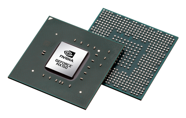
The Nvidia GeForce MX150 is a dedicated entry-level mobile graphics card for laptops based on the GP108 chip with the Pascal architecture. It was announced mid 2017 and is the mobile version of the desktop GeForce GT 1030 . It offers the same 384 shader cores and 64 Bit memory bus manufactured in 14 nm. The clock rates and performance however are a bit higher than the desktop GT 1030. Officially it is the successor to the older Maxwell based GeForce 940MX .
Currently there are two variants of the MX150, a "normal" N17S-G1-A1 with 1468 - 1531 MHz and 25 Watt TDP and a power efficient variant named N17S-LG-A1 with 936 - 1037 MHz (-32%) and 10 Watt TDP (-60%) for thin and light laptops.
The GP108 chip is manufactured in a 14 nm FinFET process at Samsung (LPP) and offers a number of new features, including support for DisplayPort 1.4 (ready), HDMI 2.0b, HDR and improved H.265 video de- and encoding (PlayReady 3.0). 4K HDR with Netflix however wont run due to the minimum 3 GB graphics memory that is required. Compared to the bigger Pascal chips, the small GP108 does not support Simultaneous Multi-Projection (SMP) for VR and G-Sync. A full list of improvements and the new Pascal desktop GPUs is available in our dedicated Pascal architecture article
The performance however is higher than the old GeForce GTX 950M with GDDR5 memory. Still modern and demanding games only run in low settings and resolutions fluently. E.g. Assassin's Creed Origins was only playable in lowest settings and 1280x720 pixels. Less demanding games like Call of Duty WW2 also ran in medium settings and Full HD fluently. See below for more and detailed gaming benchmarks.
The power efficient N17S-LG-A1 ULV variant is clearly slower than the normal one (due to the 32% lower boost clock).
The power consumption (25 Watt TDP of the chip alone) however lies on a level of the old 940MX (23 Watt). The older 950M and the new GTX 1050 are rated much higher with 40 Watt TDP. The GeForce MX150 also uses a small 23 x 23 mm package due to the small chip size.
Intel Iris Plus Graphics 645 ► remove from comparison
The Intel Iris Plus Graphics 645 (GT3e) is a processor graphics card that was first seen in the Apple MacBook Pro 13 (Entry, 2019) in mid 2019. It is similar to the Iris Plus Graphics 655 in the 28 Watt CPUs.
The so called GT3e version of the Coffee-Lake GPU still has 48 Execution Units (EUs), which can reach up to 1150 MHz depending on the model. Besides eDRAM cache, the Iris 645 can also access the system memory (2x 64 Bit DDR3L-2133/DDR4-2400) via processor interface.
The exact performance of the Iris Plus Graphics 645 depends on the CPU model, because maximum clock as well as the size of the L3 cache can differ a bit. The system memory (DDR3/DDR4) will influence the performance as well.
The fastest chips are high-clocked Core i7 models like the Core i7-8557U. Depending on the game, the Iris Plus 655 will probably be on par with a dedicated GeForce 930M or GeForce 940MX and can handle smooth gameplay in modern titles in low up to medium settings.
The reworked video engine now fully supports hardware decoding of H.265/HEVC videos. Contrary to Skylake, however, Kaby Lake can now also decode H.265/HEVC Main 10 with a 10-bit color depth as well as Google's VP9 codec. The video output is possible via DP 1.2/eDP 1.3 (up to 3840 x 2160 @60 Hz), whereas HDMI is also supported in the older 1.4a standard. An HDMI 2.0 output can be added via converter from DisplayPort. The GPU can drive up to three displays simultaneously.
The Iris Plus Graphics 645 is used for 15-Watt processor and therefore small-sized notebooks.
Intel UHD Graphics 620 NVIDIA GeForce MX150 Intel Iris Plus Graphics 645 Gen. 9.5 Series GeForce MX150 384 @ 1.47 - 1.53 GHz 64 Bit @ 6008 MHz GeForce MX130 384 @ 1.12 - 1.24 GHz 64 Bit GeForce MX110 256 @ 0.97 - 0.99 GHz 64 Bit @ 1800 MHz
Codename Kaby-Lake-Refresh GT2 N17S-G1 Kaby Lake GT3e Architecture Gen. 9.5 Pascal Gen. 9.5 Coffee Lake Pipelines 24 - unified 384 - unified 48 - unified Core Speed 300 - 1150 (Boost) MHz 1468 - 1532 (Boost) MHz 300 - 1150 (Boost) MHz Theoretical Performance 883 TFLOPS FP16, 442 TFLOPS FP32, 110.4 TFLOPS FP64 Memory Type DDR3/DDR4 GDDR5 DDR3, DDR4 Shared Memory yes no yes API DirectX 12_1, OpenGL 4.4 DirectX 12_1, OpenGL 4.5 DirectX 12_1, OpenGL 4.5 technology 14 nm 14 nm 14 nm Displays HDMI 1.4, DisplayPort 1.2 Features QuickSync Vulkan, Multi Monitor, Nvidia Optimus QuickSync Date of Announcement 01.09.2017 16.05.2017 10.07.2019 Predecessor HD Graphics 620 GeForce 940MX TMUs 24 ROPs 16 Memory Speed 6008 effective = 1502 MHz Memory Bus Width 64 Bit Max. Amount of Memory 4 GB Memory Bandwidth 40.1 GB/s Power Consumption 25 Watt (10 - 25 Watt TGP) Transistors 1.8 Billion Die Size 71 mm² PCIe 3 x4 Link to Manufacturer Page www.geforce.com Successor GeForce MX250
CPU in UHD Graphics 620 GPU Base Speed GPU Boost / Turbo Intel Core i7-10810U 6 x 1100 MHz, 15 W 300 MHz 1150 MHz Intel Core i7-10710U 6 x 1100 MHz, 15 W 300 MHz 1150 MHz Intel Core i7-10610U 4 x 1800 MHz, 15 W 300 MHz 1150 MHz » show 15 more Intel Core i7-10510U 4 x 1800 MHz, 15 W 300 MHz 1150 MHz Intel Core i5-10310U 4 x 1700 MHz, 15 W 300 MHz 1150 MHz Intel Core i7-8665U 4 x 1900 MHz, 15 W 300 MHz 1150 MHz Intel Core i7-8650U 4 x 1900 MHz, 15 W 300 MHz 1150 MHz Intel Core i5-10210U 4 x 1600 MHz, 15 W 300 MHz 1100 MHz Intel Core i7-8565U 4 x 1800 MHz, 15 W 300 MHz 1150 MHz Intel Core i5-8365U 4 x 1600 MHz, 15 W 300 MHz 1100 MHz Intel Core i5-8265U 4 x 1600 MHz, 15 W 300 MHz 1100 MHz Intel Core i7-8550U 4 x 1800 MHz, 15 W 300 MHz 1150 MHz Intel Core i5-8260U 4 x 1600 MHz, 15 W 300 MHz 1100 MHz Intel Core i3-10110U 2 x 2100 MHz, 15 W 300 MHz 1000 MHz Intel Core i5-8350U 4 x 1700 MHz, 15 W 300 MHz 1100 MHz Intel Core i5-8250U 4 x 1600 MHz, 15 W 300 MHz 1100 MHz Intel Core i3-8145U 2 x 2100 MHz, 15 W 300 MHz 1000 MHz Intel Core i3-8130U 2 x 2200 MHz, 15 W 300 MHz 1000 MHz min. - max. 300 MHz 1000 - 1150 MHz
CPU in Iris Plus Graphics 645 GPU Base Speed GPU Boost / Turbo Intel Core i7-8557U 4 x 1700 MHz, 28 W 300 MHz 1150 MHz Intel Core i5-8257U 4 x 1400 MHz, 15 W 300 MHz 1050 MHz min. - max. 300 MHz 1000 - 1150 MHz
Benchmarks Performance Rating - 3DMark 11 + Fire Strike + Time Spy - UHD Graphics 620
0.5 pt (2%)
...
...
max:
Performance Rating - 3DMark 11 + Fire Strike + Time Spy - GeForce MX150
1.6 pt (5%)
...
...
max:
3DMark - 3DMark Time Spy Score
min: 343 avg: 443.9 median: 435.5 (1%) max: 879 Points
min: 929 avg: 1101 median: 1132.5 (3%) max: 1280 Points
624 Points (2%)
3DMark - 3DMark Time Spy Graphics
min: 299 avg: 389.1 median: 380 (1%) max: 797 Points
min: 830 avg: 995 median: 1046 (3%) max: 1147 Points
550 Points (1%)
3DMark - 3DMark Ice Storm Unlimited Graphics
min: 60554 avg: 88650 median: 88745.5 (10%) max: 115515 Points
min: 178723 avg: 212534 median: 223740 (25%) max: 240298 Points
3DMark - 3DMark Ice Storm Extreme Graphics
min: 26409 avg: 42924 median: 42561 (5%) max: 59483 Points
min: 30503 avg: 57805 median: 46586.5 (6%) max: 82527 Points
3DMark - 3DMark Cloud Gate Score
min: 5358 avg: 8164 median: 8139 (9%) max: 10960 Points
min: 8464 avg: 12772 median: 12943 (14%) max: 15777 Points
3DMark - 3DMark Cloud Gate Graphics
min: 6205 avg: 9262 median: 9324 (2%) max: 16400 Points
min: 16227 avg: 19512 median: 19132 (5%) max: 22183 Points
3DMark - 3DMark Fire Strike Standard Score
min: 538 avg: 1063 median: 1071 (2%) max: 2263 Points
min: 2100 avg: 2999 median: 3104 (5%) max: 3377 Points
1736 Points (3%)
3DMark - 3DMark Fire Strike Standard Graphics
min: 557 avg: 1161 median: 1168 (1%) max: 2608 Points
min: 2323 avg: 3310 median: 3488 (4%) max: 3739 Points
1893 Points (2%)
3DMark - 3DMark Ice Storm Graphics
min: 13790 avg: 67871 median: 67131.5 (8%) max: 102010 Points
min: 31036 avg: 66344 median: 68607 (8%) max: 101641 Points
3DMark - 3DMark Sling Shot (ES 3.0) Unlimited
7727 Points (34%)
3DMark - 3DMark Sling Shot (ES 3.0) Unlimited Graphics
8007 Points (18%)
3DMark - 3DMark Sling Shot Extreme (ES 3.1) Unlimited
min: 5204 avg: 5377 median: 5376.5 (27%) max: 5549 Points
3DMark - 3DMark Sling Shot Extreme (ES 3.1) Unlimited Graphics
min: 4856 avg: 5023 median: 5023 (15%) max: 5190 Points
3DMark - 3DMark Wild Life Unlimited
min: 2133 avg: 2844 median: 2916 (1%) max: 3306 Points
3DMark - 3DMark Night Raid
min: 3967 avg: 5202 median: 5245 (5%) max: 6637 Points
3DMark - 3DMark Night Raid Graphics Score
min: 4163 avg: 5221 median: 5312 (2%) max: 6380 Points
3DMark 11 - 3DM11 Performance Score
min: 1175 avg: 1932 median: 1935.5 (3%) max: 3374 Points
min: 3028 avg: 4405 median: 4576 (6%) max: 5219 Points
3238 Points (4%)
3DMark 11 - 3DM11 Performance GPU
min: 1144 avg: 1749 median: 1744 (1%) max: 3432 Points
min: 2796 avg: 4191 median: 4494 (4%) max: 4905 Points
2985 Points (3%)
3DMark Vantage + Intel UHD Graphics 620 3DMark Vantage - 3DM Vant. Perf. total
min: 6899 avg: 7330 median: 7330 (2%) max: 7761 Points
3DM Vant. Perf. total + NVIDIA GeForce MX150
min: 7839 avg: 10992 median: 10991.5 (3%) max: 14144 Points
3DM Vant. Perf. GPU no PhysX + Intel UHD Graphics 620 3DMark Vantage - 3DM Vant. Perf. GPU no PhysX
min: 5555 avg: 5948 median: 5948 (3%) max: 6341 Points
3DM Vant. Perf. GPU no PhysX + NVIDIA GeForce MX150
min: 6377 avg: 10755 median: 10754.5 (6%) max: 15132 Points
3DMark 2001SE - 3DMark 2001 - Standard
34467 Points (36%)
34443 Points (36%)
3DMark 05 - 3DMark 05 - Standard
16972 Points (19%)
3DMark 06 3DMark 06 - Standard 1280x1024 + Intel UHD Graphics 620
min: 7653 avg: 10777 median: 10642 (14%) max: 14158 Points
3DMark 06 - Standard 1280x1024 + NVIDIA GeForce MX150
min: 12796 avg: 19251 median: 19312.5 (25%) max: 24726 Points
Unigine Valley 1.0 - Unigine Valley 1.0 DX
min: 3.9 avg: 4.7 median: 4.7 (2%) max: 5.5 fps
min: 14.6 avg: 15.7 median: 15.7 (5%) max: 16.8 fps
Unigine Heaven 3.0 - Unigine Heaven 3.0 DX 11
19.2 fps (6%)
41.8 fps (14%)
Unigine Heaven 2.1 - Heaven 2.1 high
min: 27 avg: 42 median: 42 (8%) max: 56.9 fps
SPECviewperf 12 + Intel UHD Graphics 620 SPECviewperf 12 - specvp12 sw-03
min: 17.99 avg: 23.9 median: 24.1 (6%) max: 28.71 fps
specvp12 sw-03 + NVIDIA GeForce MX150
min: 23.01 avg: 24.1 median: 24.4 (6%) max: 24.99 fps
specvp12 snx-02 + Intel UHD Graphics 620 SPECviewperf 12 - specvp12 snx-02
min: 2.49 avg: 2.7 median: 2.7 (0%) max: 2.98 fps
specvp12 snx-02 + NVIDIA GeForce MX150 min: 3.07 avg: 3.1 median: 3.1 (0%) max: 3.26 fps
specvp12 showcase-01 + Intel UHD Graphics 620 SPECviewperf 12 - specvp12 showcase-01
min: 5 avg: 6.7 median: 6.8 (1%) max: 8.35 fps
specvp12 showcase-01 + NVIDIA GeForce MX150
min: 13.22 avg: 14.3 median: 13.9 (3%) max: 15.8 fps
specvp12 mediacal-01 + Intel UHD Graphics 620 SPECviewperf 12 - specvp12 mediacal-01
min: 2.62 avg: 3.8 median: 2.9 (1%) max: 9.17 fps
specvp12 mediacal-01 + NVIDIA GeForce MX150
min: 9.81 avg: 10.6 median: 10.3 (3%) max: 11.55 fps
specvp12 maya-04 + Intel UHD Graphics 620 SPECviewperf 12 - specvp12 maya-04
min: 4.27 avg: 11.8 median: 13 (4%) max: 15.71 fps
specvp12 maya-04 + NVIDIA GeForce MX150
min: 25.1 avg: 27.8 median: 26.2 (7%) max: 32.06 fps
specvp12 energy-01 + Intel UHD Graphics 620 SPECviewperf 12 - specvp12 energy-01
min: 0.22 avg: 0.3 median: 0.2 (0%) max: 0.81 fps
specvp12 energy-01 + NVIDIA GeForce MX150 min: 0.49 avg: 0.5 median: 0.5 (0%) max: 0.56 fps
specvp12 creo-01 + Intel UHD Graphics 620 SPECviewperf 12 - specvp12 creo-01
min: 7.9 avg: 12.4 median: 12.9 (5%) max: 14.42 fps
specvp12 creo-01 + NVIDIA GeForce MX150
min: 11.08 avg: 11.3 median: 11.2 (4%) max: 11.52 fps
specvp12 catia-04 + Intel UHD Graphics 620 SPECviewperf 12 - specvp12 catia-04
min: 7.38 avg: 13.3 median: 13.8 (2%) max: 16.55 fps
specvp12 catia-04 + NVIDIA GeForce MX150
min: 16.44 avg: 17.1 median: 16.9 (3%) max: 17.85 fps
specvp12 3dsmax-05 + Intel UHD Graphics 620 SPECviewperf 12 - specvp12 3dsmax-05
min: 10.98 avg: 13.2 median: 13 (2%) max: 15.22 fps
specvp12 3dsmax-05 + NVIDIA GeForce MX150
min: 22.02 avg: 23 median: 23 (4%) max: 23.92 fps
SPECviewperf 13 specvp13 sw-04 + Intel UHD Graphics 620 SPECviewperf 13 - specvp13 sw-04
min: 27.99 avg: 32.4 median: 31.9 (9%) max: 37.6 fps
specvp13 sw-04 + NVIDIA GeForce MX150
35.3 fps (9%)
specvp13 snx-03 + Intel UHD Graphics 620 SPECviewperf 13 - specvp13 snx-03
min: 4.37 avg: 4.9 median: 4.9 (1%) max: 5.37 fps
specvp13 snx-03 + NVIDIA GeForce MX150
5.9 fps (1%)
specvp13 showcase-02 + Intel UHD Graphics 620 SPECviewperf 13 - specvp13 showcase-02
min: 4.99 avg: 6.7 median: 6.8 (1%) max: 8.34 fps
specvp13 showcase-02 + NVIDIA GeForce MX150
15.7 fps (3%)
specvp13 medical-02 + Intel UHD Graphics 620 SPECviewperf 13 - specvp13 medical-02
min: 1.96 avg: 2.1 median: 2.2 (0%) max: 2.26 fps
specvp13 medical-02 + NVIDIA GeForce MX150
8.5 fps (2%)
specvp13 maya-05 + Intel UHD Graphics 620 SPECviewperf 13 - specvp13 maya-05
min: 15.66 avg: 19.4 median: 19.6 (2%) max: 22.97 fps
specvp13 maya-05 + NVIDIA GeForce MX150
54.2 fps (6%)
specvp13 energy-02 + Intel UHD Graphics 620 SPECviewperf 13 - specvp13 energy-02
min: 0.21 avg: 1.3 median: 1.1 (0%) max: 2.85 fps
specvp13 creo-02 + Intel UHD Graphics 620 SPECviewperf 13 - specvp13 creo-02
min: 15.15 avg: 17.1 median: 17 (2%) max: 18.88 fps
specvp13 creo-02 + NVIDIA GeForce MX150
27.1 fps (4%)
specvp13 catia-05 + Intel UHD Graphics 620 SPECviewperf 13 - specvp13 catia-05
min: 17.43 avg: 20.2 median: 20 (2%) max: 23.37 fps
specvp13 catia-05 + NVIDIA GeForce MX150
25.8 fps (3%)
specvp13 3dsmax-06 + Intel UHD Graphics 620 SPECviewperf 13 - specvp13 3dsmax-06
min: 10.82 avg: 13.1 median: 13.1 (2%) max: 15.01 fps
specvp13 3dsmax-06 + NVIDIA GeForce MX150
23.3 fps (4%)
Cinebench R10 Cinebench R10 Shading (32bit) + Intel UHD Graphics 620 Cinebench R10 - Cinebench R10 Shading (32bit)
min: 5525 avg: 8182 median: 8194 (6%) max: 20592 Points
Cinebench R10 Shading (32bit) + NVIDIA GeForce MX150
min: 3328 avg: 6014 median: 6526.5 (5%) max: 10464 Points
Cinebench R11.5 Cinebench R11.5 OpenGL 64 Bit + Intel UHD Graphics 620 Cinebench R11.5 - Cinebench R11.5 OpenGL 64 Bit
min: 23.54 avg: 41.3 median: 41.3 (14%) max: 54.5 fps
Cinebench R11.5 OpenGL 64 Bit + NVIDIA GeForce MX150
min: 1.45 avg: 62.6 median: 65.2 (23%) max: 77.9 fps
Cinebench R15 + Intel UHD Graphics 620 Cinebench R15 - Cinebench R15 OpenGL 64 Bit
min: 30.56 avg: 49.6 median: 48.8 (3%) max: 97.8 fps
Cinebench R15 OpenGL 64 Bit + NVIDIA GeForce MX150
min: 59.7 avg: 92.8 median: 94.1 (5%) max: 111.1 fps
Cinebench R15 OpenGL 64 Bit + Intel Iris Plus Graphics 645
min: 55.3 avg: 67.1 median: 67.1 (4%) max: 78.9 fps
Cinebench R15 OpenGL Ref. Match 64 Bit + Intel UHD Graphics 620 Cinebench R15 - Cinebench R15 OpenGL Ref. Match 64 Bit
min: 47.63 avg: 97.2 median: 97.8 (98%) max: 98.8 %
Cinebench R15 OpenGL Ref. Match 64 Bit + NVIDIA GeForce MX150
99.6 % (100%)
Cinebench R15 OpenGL Ref. Match 64 Bit + Intel Iris Plus Graphics 645
min: 97.8 avg: 98.6 median: 98.6 (99%) max: 99.3 %
GFXBench - GFXBench 5.0 Aztec Ruins High Tier Offscreen
min: 9.9 avg: 12 median: 10 (2%) max: 16 fps
20.2 fps (4%)
GFXBench - GFXBench 5.0 Aztec Ruins Normal Tier Offscreen
min: 26 avg: 26.7 median: 27 (2%) max: 27 fps
53.4 fps (4%)
GFXBench - GFXBench Car Chase Offscreen
min: 24 avg: 28.3 median: 27.5 (3%) max: 34.4 fps
min: 52.9 avg: 63 median: 61.8 (7%) max: 75.4 fps
GFXBench 3.1 - GFXBench Manhattan ES 3.1 Offscreen
min: 22 avg: 36.6 median: 39.8 (1%) max: 45.7 fps
min: 85.1 avg: 94.6 median: 90.9 (2%) max: 111.5 fps
69.6 fps (1%)
GFXBench 3.0 - GFXBench 3.0 Manhattan Offscreen
min: 0 avg: 48.8 median: 58.9 (3%) max: 70.7 fps
min: 121.5 avg: 129.5 median: 123.9 (7%) max: 148.7 fps
101.8 fps (6%)
GFXBench (DX / GLBenchmark) 2.7 + Intel UHD Graphics 620 GFXBench (DX / GLBenchmark) 2.7 - GFXBench T-Rex HD Offscreen C24Z16
min: 73.3 avg: 114.4 median: 119.1 (1%) max: 135 fps
GFXBench T-Rex HD Offscreen C24Z16 + NVIDIA GeForce MX150
min: 203 avg: 225.7 median: 207.9 (2%) max: 283.9 fps
GFXBench T-Rex HD Offscreen C24Z16 + Intel Iris Plus Graphics 645
198.3 fps (2%)
Basemark GPU 1.2 - Basemark GPU 1.2 Vulkan Official Medium Offscreen 1080
51.6 fps (0%)
140 fps (1%)
Basemark GPU 1.2 - Basemark GPU 1.2 Vulkan Official High Offscreen 2160
4.4 fps (1%)
Geekbench 6.2 - Geekbench 6.2 GPU OpenCL
4989 Points (1%)
Geekbench 6.2 - Geekbench 6.2 GPU Vulkan
5447 Points (2%)
LuxMark v2.0 64Bit - LuxMark v2.0 Room GPU
min: 109 avg: 279.4 median: 291 (1%) max: 336 Samples/s
min: 415 avg: 489.7 median: 437.5 (2%) max: 769 Samples/s
LuxMark v2.0 64Bit - LuxMark v2.0 Sala GPU
min: 266 avg: 641 median: 653 (1%) max: 755 Samples/s
min: 734 avg: 879 median: 773.5 (1%) max: 1451 Samples/s
ComputeMark v2.1 - ComputeMark v2.1 Result
min: 631 avg: 927 median: 937 (1%) max: 1023 Points
min: 2256 avg: 2544 median: 2581 (3%) max: 2856 Points
PassMark PerformanceTest Mobile V1 - PerformanceTest Mobile V1 2D Graphics Tests
99897 Points (100%)
PassMark PerformanceTest Mobile V1 - PerformanceTest Mobile V1 3D Graphics Tests
0 Points (0%)
Power Consumption - Furmark Stress Test Power Consumption - external Monitor *
min: 20.7 avg: 30.5 median: 29.2 (4%) max: 46.6 Watt
min: 25.9 avg: 44.5 median: 42.6 (6%) max: 66.8 Watt
Power Consumption - The Witcher 3 Power Consumption - external Monitor *
min: 19.6 avg: 27.9 median: 27.2 (4%) max: 35 Watt
min: 29.5 avg: 40.5 median: 39.4 (5%) max: 53.1 Watt
Power Consumption - Witcher 3 Power Consumption *
min: 22.6 avg: 31.9 median: 31.7 (7%) max: 43 Watt
min: 32.8 avg: 48.6 median: 50.6 (11%) max: 67.6 Watt
Power Consumption - Witcher 3 ultra Power Efficiency
min: 0.1315 avg: 0.2 median: 0.2 (21%) max: 0.2876 fps per Watt
min: 0.1729 avg: 0.2 median: 0.2 (23%) max: 0.3333 fps per Watt
Power Consumption - Witcher 3 ultra Power Efficiency - external Monitor
min: 0.1611 avg: 0.2 median: 0.2 (20%) max: 0.3316 fps per Watt
min: 0.228 avg: 0.3 median: 0.3 (23%) max: 0.3288 fps per Watt
Emissions Witcher 3 Fan Noise + Intel UHD Graphics 620 Emissions - Witcher 3 Fan Noise
min: 27.3 avg: 32.3 median: 33 (53%) max: 36 dB(A)
Witcher 3 Fan Noise + NVIDIA GeForce MX150
min: 32.5 avg: 39.6 median: 40 (64%) max: 47.9 dB(A)
Clock Speed - GPU Clock Witcher 3 ultra
min: 986 avg: 1033 median: 1024 (40%) max: 1097 MHz
min: 1290 avg: 1447 median: 1438.5 (56%) max: 1620 MHz
Clock Speed - GPU Clock Speed Furmark
min: 764 avg: 982 median: 960.5 (38%) max: 1142 MHz
min: 813 avg: 1056 median: 1177 (47%) max: 1177 MHz
Average Benchmarks Intel UHD Graphics 620 → 100% n=11 Average Benchmarks NVIDIA GeForce MX150 → 230% n=11 Average Benchmarks Intel Iris Plus Graphics 645 → 155% n=11
- Range of benchmark values for this graphics card
- Average benchmark values for this graphics card
* Smaller numbers mean a higher performance
1 This benchmark is not used for the average calculation
Game Benchmarks The following benchmarks stem from our benchmarks of review laptops. The performance depends on the used graphics memory, clock rate, processor, system settings, drivers, and operating systems. So the results don't have to be representative for all laptops with this GPU. For detailed information on the benchmark results, click on the fps number.
100%
UHD Graphics 620:
5.5 [X] Lenovo Ideapad S540-14IML Intel Core i7-10510U 1.8GHz
UHD Graphics 620
min:
2.61 fps, P0.1:
2.62 fps, P1:
2.72 fps, max:
99.2 fps
fps
100%
UHD Graphics 620:
15.8 [X] Lenovo Ideapad S540-14IML Intel Core i7-10510U 1.8GHz
UHD Graphics 620
fps
100%
UHD Graphics 620:
10.5 [X] Lenovo Ideapad S540-14IML Intel Core i7-10510U 1.8GHz
UHD Graphics 620
fps
100%
UHD Graphics 620:
16.5 [X] Lenovo Ideapad S540-14IML Intel Core i7-10510U 1.8GHz
UHD Graphics 620
min:
1.953 fps, P0.1:
2.23 fps, P1:
5.61 fps, max:
653 fps
fps
100%
UHD Graphics 620:
16.5 [X] Lenovo Ideapad S540-14IML Intel Core i7-10510U 1.8GHz
UHD Graphics 620
min:
10.6 fps, P0.1:
10.7 fps, P1:
11.8 fps, max:
36.8 fps
fps
100%
UHD Graphics 620:
5.7 [X] Lenovo Ideapad S540-14IML Intel Core i7-10510U 1.8GHz
UHD Graphics 620
min:
3.96 fps, P0.1:
3.97 fps, P1:
4.13 fps, max:
8.29 fps
fps
100%
UHD Graphics 620:
5.1 [X] Lenovo Ideapad S540-14IML 2.02
Intel Core i7-10510U 1.8GHz
UHD Graphics 620
min:
3.75 fps, max:
6.94 fps
fps
100%
UHD Graphics 620:
6.6 [X] Lenovo Ideapad S540-14IML Intel Core i7-10510U 1.8GHz
UHD Graphics 620
min:
3.16 fps, P0.1:
3.17 fps, P1:
3.21 fps, max:
89.3 fps
fps
100%
UHD Graphics 620:
8.2 [X] Lenovo Ideapad S540-14IML Intel Core i7-10510U 1.8GHz
UHD Graphics 620
min:
4.67 fps, P0.1:
4.98 fps, P1:
6.95 fps, max:
18.2 fps
fps
100%
UHD Graphics 620:
5.3 [X] Lenovo Ideapad S540-14IML Intel Core i7-10510U 1.8GHz
UHD Graphics 620
min:
4.6 fps, P0.1:
4.63 fps, P1:
4.75 fps, max:
6.31 fps
fps
100%
UHD Graphics 620:
9.5 [X] Lenovo Ideapad S540-14IML Intel Core i7-10510U 1.8GHz
UHD Graphics 620
min:
7.33 fps, P0.1:
7.39 fps, P1:
7.73 fps, max:
11.6 fps
fps
100%
UHD Graphics 620:
9.4 [X] Lenovo Ideapad S540-14IML Intel Core i7-10510U 1.8GHz
UHD Graphics 620
min:
3.21 fps, P0.1:
3.48 fps, P1:
4.81 fps, max:
91.9 fps
fps
100%
UHD Graphics 620:
7 [X] Lenovo Ideapad S540-14IML Intel Core i7-10510U 1.8GHz
UHD Graphics 620
P0.1:
2.9 fpsP1:
4.5 fps
fps
100%
UHD Graphics 620:
4.4 [X] Lenovo Ideapad S540-14IML Intel Core i7-10510U 1.8GHz
UHD Graphics 620
min:
1.148 fps, P0.1:
1.192 fps, P1:
2.61 fps, max:
25.3 fps
fps
100%
UHD Graphics 620:
7.7 [X] Lenovo Ideapad S540-14IML Intel Core i7-10510U 1.8GHz
UHD Graphics 620
min:
6.91 fps, P0.1:
6.94 fps, P1:
7.1 fps, max:
8.55 fps
fps
100%
UHD Graphics 620:
3.7 [X] Lenovo Ideapad S540-14IML Intel Core i7-10510U 1.8GHz
UHD Graphics 620
min:
3.04 fps, P0.1:
3.04 fps, P1:
3.06 fps, max:
4.78 fps
fps
100%
UHD Graphics 620:
10.6 [X] HP Probook 470 G5 4QW96EA Intel Core i7-8550U 1.8GHz
UHD Graphics 620
min:
4.45 fps, P0.1:
4.56 fps, P1:
5.04 fps, max:
74.4 fps
fps
100%
UHD Graphics 620:
5.2 [X] HP Probook 470 G5 4QW96EA Intel Core i7-8550U 1.8GHz
UHD Graphics 620
fps
100%
UHD Graphics 620:
7 [X] HP Probook 470 G5 4QW96EA Intel Core i7-8550U 1.8GHz
UHD Graphics 620
min:
4 fps
fps
100%
UHD Graphics 620:
5 [X] Lenovo Ideapad S540-14IML Intel Core i7-10510U 1.8GHz
UHD Graphics 620
min:
3.53 fps, P0.1:
3.53 fps, P1:
3.73 fps, max:
6.58 fps
fps
GeForce MX150:
14.5 [X] Honor Magicbook Intel Core i5-8250U 1.6GHz
GeForce MX150
min:
6.03 fps, P0.1:
6.28 fps, P1:
10 fps, max:
72.1 fps
fps
GeForce MX150:
9.1 [X] Honor Magicbook Intel Core i5-8250U 1.6GHz
GeForce MX150
min:
4.14 fps, P0.1:
4.15 fps, P1:
5.09 fps, max:
60.2 fps
fps
GeForce MX150:
6.7 [X] Honor Magicbook Intel Core i5-8250U 1.6GHz
GeForce MX150
min:
3.21 fps, P0.1:
3.27 fps, P1:
3.74 fps, max:
88.8 fps
fps
GeForce MX150:
27.4 [X] Honor Magicbook 913427
Intel Core i5-8250U 1.6GHz
GeForce MX150
min:
22 fps, P1:
21 fps, max:
31 fps
fps
GeForce MX150:
19.3 [X] Honor Magicbook 913427
Intel Core i5-8250U 1.6GHz
GeForce MX150
min:
15 fps, P1:
15 fps, max:
23 fps
fps
100%
UHD Graphics 620:
16 [X] HP Probook 470 G5 4QW96EA Intel Core i7-8550U 1.8GHz
UHD Graphics 620
min:
3.68 fps, P0.1:
5.7 fps, P1:
12.8 fps, max:
63.1 fps
fps
100%
UHD Graphics 620:
9.9 [X] HP Probook 470 G5 4QW96EA Intel Core i7-8550U 1.8GHz
UHD Graphics 620
min:
3.32 fps, P0.1:
3.37 fps, P1:
4.83 fps, max:
52.1 fps
fps
100%
UHD Graphics 620:
5.1 [X] Honor Magicbook Intel Core i5-8250U 1.6GHz
UHD Graphics 620
min:
2.53 fps, P0.1:
2.56 fps, P1:
2.74 fps, max:
36.5 fps
fps
260%
GeForce MX150:
13.2 [X] Honor Magicbook Intel Core i5-8250U 1.6GHz
GeForce MX150
min:
5.48 fps, P0.1:
5.91 fps, P1:
6.58 fps, max:
90.8 fps
fps
100%
UHD Graphics 620:
7 7.9 [X] Honor Magicbook Intel Core i5-8250U 1.6GHz
UHD Graphics 620
~ 7 fps
267%
GeForce MX150:
18.7 fps
100%
UHD Graphics 620:
5.1 fps
100%
UHD Graphics 620:
3.3 fps
100%
UHD Graphics 620:
5.7 [X] Honor Magicbook 1.5
Intel Core i5-8250U 1.6GHz
UHD Graphics 620
min:
2.65 fps, max:
17.8 fps
fps
GeForce MX150:
10.9 [X] Honor Magicbook 1.5
Intel Core i5-8250U 1.6GHz
GeForce MX150
min:
7.7 fps, max:
16.6 fps
fps
GeForce MX150:
16.7 [X] Honor Magicbook Intel Core i5-8250U 1.6GHz
GeForce MX150
min:
2.64 fps, P0.1:
2.74 fps, P1:
9.18 fps, max:
45.6 fps
fps
100%
UHD Graphics 620:
17 [X] Honor Magicbook Intel Core i5-8250U 1.6GHz
UHD Graphics 620
min:
13 fps, max:
23 fps
fps
244%
GeForce MX150:
41.5 fps
100%
UHD Graphics 620:
11.5 [X] Honor Magicbook Intel Core i5-8250U 1.6GHz
UHD Graphics 620
min:
9 fps, max:
18 fps
fps
100%
UHD Graphics 620:
6.3 (!) [X] Honor Magicbook Intel Core i5-8250U 1.6GHz
UHD Graphics 620
min:
2.33 fps, P0.1:
2.35 fps, P1:
4.7 fps, max:
29.6 fps
fps
369%
GeForce MX150:
23.2 [X] Honor Magicbook Intel Core i5-8250U 1.6GHz
GeForce MX150
min:
9.59 fps, P0.1:
10.6 fps, P1:
16.5 fps, max:
39.2 fps
fps
100%
UHD Graphics 620:
10 [X] HP Probook 470 G5 4QW96EA Intel Core i7-8550U 1.8GHz
UHD Graphics 620
min:
6 fps, max:
12 fps
fps
200%
GeForce MX150:
20 fps
GeForce MX150:
11.8 [X] Honor Magicbook Intel Core i5-8250U 1.6GHz
GeForce MX150
min:
4.76 fps, P0.1:
4.9 fps, P1:
6.52 fps, max:
17.1 fps
fps
GeForce MX150:
1.9 [X] Honor Magicbook Intel Core i5-8250U 1.6GHz
GeForce MX150
min:
1.441 fps, P0.1:
1.444 fps, P1:
1.499 fps, max:
3.07 fps
fps
100%
UHD Graphics 620:
33 (!) [X] HP Probook 470 G5 4QW96EA Intel Core i7-8550U 1.8GHz
UHD Graphics 620
min:
2.77 fps, P0.1:
3.58 fps, P1:
6.77 fps, max:
122.9 fps
fps
GeForce MX150:
31.6 [X] Honor Magicbook Intel Core i5-8250U 1.6GHz
GeForce MX150
min:
5.59 fps, P0.1:
8.96 fps, P1:
13.6 fps, max:
85.1 fps
fps
GeForce MX150:
7.8 [X] Honor Magicbook Intel Core i5-8250U 1.6GHz
GeForce MX150
min:
3.61 fps, P0.1:
3.69 fps, P1:
4.77 fps, max:
59.7 fps
fps
GeForce MX150:
1.9 [X] Honor Magicbook Intel Core i5-8250U 1.6GHz
GeForce MX150
min:
1.32 fps, P0.1:
1.328 fps, P1:
1.372 fps, max:
5.99 fps
fps
100%
UHD Graphics 620:
10 [X] HP Probook 470 G5 4QW96EA Intel Core i7-8550U 1.8GHz
UHD Graphics 620
min:
6 fps, max:
13 fps
fps
100%
UHD Graphics 620:
19.5 [X] HP Probook 470 G5 4QW96EA Intel Core i7-8550U 1.8GHz
UHD Graphics 620
min:
4.99 fps, P0.1:
6.88 fps, P1:
14 fps, max:
110.8 fps
fps
100%
UHD Graphics 620:
15 [X] HP Probook 470 G5 4QW96EA Intel Core i7-8550U 1.8GHz
UHD Graphics 620
min:
2.42 fps, P0.1:
3.46 fps, P1:
11.2 fps, max:
67.5 fps
fps
100%
UHD Graphics 620:
9.2 [X] HP Probook 470 G5 4QW96EA Intel Core i7-8550U 1.8GHz
UHD Graphics 620
min:
1.426 fps, P0.1:
1.733 fps, P1:
4.24 fps, max:
27.5 fps
fps
GeForce MX150:
0 (!) [X] Honor Magicbook Intel Core i5-8250U 1.6GHz
GeForce MX150
fps
100%
UHD Graphics 620:
28 32 [X] Honor Magicbook 797778
Intel Core i5-8250U 1.6GHz
UHD Graphics 620
min:
25 fps, P1:
25 fps, max:
37 fps
~ 30 fps
200%
GeForce MX150:
59.9 [X] Honor Magicbook 797778
Intel Core i5-8250U 1.6GHz
GeForce MX150
min:
57 fps, P1:
37 fps, max:
60 fps
fps
100%
UHD Graphics 620:
12.2 fps
225%
GeForce MX150:
27.5 [X] Honor Magicbook 797778
Intel Core i5-8250U 1.6GHz
GeForce MX150
min:
11 fps, P1:
20 fps, max:
34 fps
fps
100%
UHD Graphics 620:
9.2 fps
236%
GeForce MX150:
21.8 [X] Honor Magicbook 797778
Intel Core i5-8250U 1.6GHz
GeForce MX150
min:
16 fps, P1:
16 fps, max:
26 fps
fps
100%
UHD Graphics 620:
36.9 [X] HP Probook 470 G5 4QW96EA Intel Core i7-8550U 1.8GHz
UHD Graphics 620
min:
24.2 fps, P0.1:
24.4 fps, P1:
27.4 fps, max:
48.3 fps
fps
100%
UHD Graphics 620:
20.2 [X] HP Probook 470 G5 4QW96EA Intel Core i7-8550U 1.8GHz
UHD Graphics 620
min:
16.3 fps, P0.1:
16.4 fps, P1:
16.6 fps, max:
24 fps
fps
100%
UHD Graphics 620:
16.9 [X] HP Probook 470 G5 4QW96EA Intel Core i7-8550U 1.8GHz
UHD Graphics 620
min:
13.7 fps, P0.1:
13.8 fps, P1:
14.1 fps, max:
20 fps
fps
100%
UHD Graphics 620:
11 [X] Honor Magicbook Intel Core i5-8250U 1.6GHz
UHD Graphics 620
min:
0.902 fps, P0.1:
0.913 fps, P1:
7.14 fps, max:
34.9 fps
fps
292%
GeForce MX150:
32.1 [X] Honor Magicbook Intel Core i5-8250U 1.6GHz
GeForce MX150
min:
2 fps, P0.1:
2.46 fps, P1:
7.36 fps, max:
86.6 fps
fps
GeForce MX150:
19.1 [X] Honor Magicbook Intel Core i5-8250U 1.6GHz
GeForce MX150
min:
6.3 fps, P0.1:
8.2 fps, P1:
11.9 fps, max:
55.3 fps
fps
100%
UHD Graphics 620:
22.6 [X] HP Probook 470 G5 4QW96EA Intel Core i7-8550U 1.8GHz
UHD Graphics 620
min:
6.25 fps, P0.1:
6.72 fps, P1:
15.1 fps, max:
46.7 fps
fps
100%
UHD Graphics 620:
11.8 [X] HP Probook 470 G5 4QW96EA Intel Core i7-8550U 1.8GHz
UHD Graphics 620
min:
0.626 fps, P0.1:
1.067 fps, P1:
8.75 fps, max:
21.7 fps
fps
100%
UHD Graphics 620:
12.2 [X] Honor Magicbook Intel Core i5-8250U 1.6GHz
UHD Graphics 620
min:
3.26 fps, P0.1:
7.04 fps, P1:
8.56 fps, max:
17.9 fps
fps
195%
GeForce MX150:
23.8 [X] Honor Magicbook Intel Core i5-8250U 1.6GHz
GeForce MX150
min:
18.6 fps, P0.1:
18.6 fps, P1:
19.2 fps, max:
33.5 fps
fps
100%
UHD Graphics 620:
21.9 [X] Honor Magicbook Intel Core i5-8250U 1.6GHz
UHD Graphics 620
min:
3.55 fps, P0.1:
4.51 fps, P1:
14.7 fps, max:
55.2 fps
fps
197%
GeForce MX150:
43.1 [X] Honor Magicbook Intel Core i5-8250U 1.6GHz
GeForce MX150
min:
15.1 fps, P0.1:
15.2 fps, P1:
23.7 fps, max:
73.3 fps
fps
GeForce MX150:
25 [X] Honor Magicbook Intel Core i5-8250U 1.6GHz
GeForce MX150
min:
8.29 fps, P0.1:
8.31 fps, P1:
10.7 fps, max:
63.1 fps
fps
GeForce MX150:
15.8 [X] Honor Magicbook Intel Core i5-8250U 1.6GHz
GeForce MX150
min:
3.82 fps, P0.1:
4.32 fps, P1:
6.59 fps, max:
59.4 fps
fps
GeForce MX150:
12.8 [X] Honor Magicbook Intel Core i5-8250U 1.6GHz
GeForce MX150
min:
2.79 fps, P0.1:
3.05 fps, P1:
4.26 fps, max:
65 fps
fps
GeForce MX150:
11.3 [X] Honor Magicbook Intel Core i5-8250U 1.6GHz
GeForce MX150
min:
3.52 fps, P0.1:
3.54 fps, P1:
4.56 fps, max:
38.2 fps
fps
100%
UHD Graphics 620:
15.7 [X] Honor Magicbook Intel Core i5-8250U 1.6GHz
UHD Graphics 620
fps
268%
GeForce MX150:
42 fps
GeForce MX150:
9.9 (!) [X] Honor Magicbook Intel Core i5-8250U 1.6GHz
GeForce MX150
fps
UHD Graphics 620:
0 (!) [X] Honor Magicbook Intel Core i5-8250U 1.6GHz
UHD Graphics 620
fps
GeForce MX150:
18.3 [X] Honor Magicbook Intel Core i5-8250U 1.6GHz
GeForce MX150
min:
9.23 fps, P0.1:
9.95 fps, P1:
13.8 fps, max:
37.5 fps
fps
GeForce MX150:
7.8 [X] Honor Magicbook Intel Core i5-8250U 1.6GHz
GeForce MX150
min:
5.21 fps, P0.1:
5.3 fps, P1:
6.13 fps, max:
10.7 fps
fps
100%
UHD Graphics 620:
11 [X] Honor Magicbook Intel Core i5-8250U 1.6GHz
UHD Graphics 620
min:
4 fps, max:
17 fps
fps
291%
GeForce MX150:
32 fps
100%
UHD Graphics 620:
15.4 [X] HP Probook 470 G5 4QW96EA Intel Core i7-8550U 1.8GHz
UHD Graphics 620
min:
5.02 fps, P0.1:
5.07 fps, P1:
10.7 fps, max:
26 fps
fps
100%
UHD Graphics 620:
0 (!) [X] Honor Magicbook Intel Core i5-8250U 1.6GHz
UHD Graphics 620
10 [X] HP Probook 470 G5 4QW96EA Intel Core i7-8550U 1.8GHz
UHD Graphics 620
min:
6 fps, max:
26 fps
~ 5 fps
300%
GeForce MX150:
15 [X] Honor Magicbook Intel Core i5-8250U 1.6GHz
GeForce MX150
min:
4 fps, P0.1:
5 fps, P1:
8 fps, max:
64 fps
fps
UHD Graphics 620:
0 (!) [X] Honor Magicbook Intel Core i5-8250U 1.6GHz
UHD Graphics 620
fps
GeForce MX150:
35.3 [X] Honor Magicbook Intel Core i5-8250U 1.6GHz
GeForce MX150
min:
15.8 fps, P0.1:
20.8 fps, P1:
29.1 fps, max:
60.7 fps
fps
GeForce MX150:
10.9 [X] Honor Magicbook Intel Core i5-8250U 1.6GHz
GeForce MX150
min:
7.6 fps, P0.1:
7.8 fps, P1:
9.3 fps, max:
12.8 fps
fps
UHD Graphics 620:
0 (!) [X] Honor Magicbook Intel Core i5-8250U 1.6GHz
UHD Graphics 620
fps
GeForce MX150:
26.9 [X] Honor Magicbook Intel Core i5-8250U 1.6GHz
GeForce MX150
min:
15.51 fps, P1:
18.5 fps, max:
71.61 fps
fps
GeForce MX150:
14.1 [X] Honor Magicbook Intel Core i5-8250U 1.6GHz
GeForce MX150
min:
9.02 fps, P1:
9.72 fps, max:
22.48 fps
fps
GeForce MX150:
11.1 [X] Honor Magicbook Intel Core i5-8250U 1.6GHz
GeForce MX150
min:
6.39 fps, P1:
8.17 fps, max:
36.27 fps
fps
100%
UHD Graphics 620:
0 (!) [X] Honor Magicbook Intel Core i5-8250U 1.6GHz
UHD Graphics 620
57.6 [X] SCHENKER Office 15 Intel Core i5-10210U 1.6GHz
UHD Graphics 620
~ 29 fps
100%
UHD Graphics 620:
29.5 [X] SCHENKER Office 15 Intel Core i5-10210U 1.6GHz
UHD Graphics 620
fps
GeForce MX150:
56.1 [X] Honor Magicbook Intel Core i5-8250U 1.6GHz
GeForce MX150
min:
25.1 fps, P1:
43.5 fps, max:
115 fps
fps
UHD Graphics 620:
0 (!) [X] Honor Magicbook Intel Core i5-8250U 1.6GHz
UHD Graphics 620
fps
GeForce MX150:
103 [X] Honor Magicbook 1.5.4.5
Intel Core i5-8250U 1.6GHz
GeForce MX150
min:
11.5 fps, P1:
60.3 fps, max:
156 fps
fps
GeForce MX150:
47.4 [X] Honor Magicbook 1.5.4.5
Intel Core i5-8250U 1.6GHz
GeForce MX150
min:
22.9 fps, P1:
36.1 fps, max:
127 fps
fps
GeForce MX150:
37.7 [X] Honor Magicbook 1.5.4.5
Intel Core i5-8250U 1.6GHz
GeForce MX150
min:
19.5 fps, P1:
30.7 fps, max:
88.6 fps
fps
GeForce MX150:
21.7 [X] Honor Magicbook 1.5.4.5
Intel Core i5-8250U 1.6GHz
GeForce MX150
min:
16.7 fps, P1:
18.8 fps, max:
33.8 fps
fps
100%
UHD Graphics 620:
11.2 [X] Honor Magicbook Intel Core i5-8250U 1.6GHz
UHD Graphics 620
min:
6.4 fps, P1:
7.77 fps, max:
24.7 fps
fps
329%
GeForce MX150:
36.8 [X] Honor Magicbook 1.5.4.5
Intel Core i5-8250U 1.6GHz
GeForce MX150
min:
16.5 fps, P1:
25.1 fps, max:
76 fps
fps
GeForce MX150:
16.1 [X] Honor Magicbook 1.5.4.5
Intel Core i5-8250U 1.6GHz
GeForce MX150
min:
12 fps, P1:
13.9 fps, max:
23.7 fps
fps
100%
UHD Graphics 620:
19.4 [X] SCHENKER Office 15 Intel Core i5-10210U 1.6GHz
UHD Graphics 620
min:
1.375 fps, P0.1:
3.31 fps, P1:
5.46 fps, max:
87.3 fps
fps
0%
GeForce MX150:
0 (!) [X] Honor Magicbook Intel Core i5-8250U 1.6GHz
GeForce MX150
fps
100%
UHD Graphics 620:
4.3 [X] SCHENKER Office 15 Intel Core i5-10210U 1.6GHz
UHD Graphics 620
min:
0.658 fps, P0.1:
0.766 fps, P1:
1.776 fps, max:
28.9 fps
fps
100%
UHD Graphics 620:
10.5 [X] Honor Magicbook Intel Core i5-8250U 1.6GHz
UHD Graphics 620
min:
3.2 fps, P1:
5.3 fps, max:
19.1 fps
fps
261%
GeForce MX150:
27.4 [X] Honor Magicbook Intel Core i5-8250U 1.6GHz
GeForce MX150
min:
7.5 fps, P1:
15.7 fps, max:
42.7 fps
fps
GeForce MX150:
10.4 [X] Honor Magicbook Intel Core i5-8250U 1.6GHz
GeForce MX150
min:
1 fps, P1:
6.2 fps, max:
30 fps
fps
100%
UHD Graphics 620:
0 (!) [X] Honor Magicbook Intel Core i5-8250U 1.6GHz
UHD Graphics 620
7 [X] SCHENKER Office 15 Intel Core i5-10210U 1.6GHz
UHD Graphics 620
max:
19 fps
~ 4 fps
650%
GeForce MX150:
26 [X] Honor Magicbook Intel Core i5-8250U 1.6GHz
GeForce MX150
min:
1 fps, P1:
10 fps, max:
56 fps
fps
GeForce MX150:
12 [X] Honor Magicbook Intel Core i5-8250U 1.6GHz
GeForce MX150
min:
3 fps, P1:
7 fps, max:
32 fps
fps
100%
UHD Graphics 620:
12.5 [X] SCHENKER Office 15 Intel Core i5-10210U 1.6GHz
UHD Graphics 620
fps
100%
UHD Graphics 620:
8.3 [X] SCHENKER Office 15 Intel Core i5-10210U 1.6GHz
UHD Graphics 620
fps
100%
UHD Graphics 620:
25.5 25.8 [X] Honor Magicbook 746942
Intel Core i5-8250U 1.6GHz
UHD Graphics 620
min:
7 fps, max:
31 fps
28 29.2 [X] Honor Magicbook 666824
Intel Core i5-8250U 1.6GHz
UHD Graphics 620
min:
15 fps, max:
35 fps
~ 27 fps
100%
UHD Graphics 620:
11.1 [X] Honor Magicbook 746942
Intel Core i5-8250U 1.6GHz
UHD Graphics 620
min:
1 fps, max:
14 fps
11.3 13 13.5 [X] Honor Magicbook 666824
Intel Core i5-8250U 1.6GHz
UHD Graphics 620
min:
9 fps, max:
16 fps
~ 12 fps
100%
UHD Graphics 620:
8.6 [X] Honor Magicbook 746942
Intel Core i5-8250U 1.6GHz
UHD Graphics 620
max:
10 fps
10 10.2 [X] Honor Magicbook 666824
Intel Core i5-8250U 1.6GHz
UHD Graphics 620
min:
7 fps, max:
11 fps
~ 10 fps
100%
UHD Graphics 620:
5.3 fps
100%
UHD Graphics 620:
80.3 [X] Honor Magicbook Intel Core i5-8250U 1.6GHz
UHD Graphics 620
min:
49 fps, max:
115 fps
fps
151%
GeForce MX150:
121 fps
100%
UHD Graphics 620:
40.1 [X] Honor Magicbook Intel Core i5-8250U 1.6GHz
UHD Graphics 620
min:
32 fps, max:
52 fps
fps
249%
GeForce MX150:
99.8 fps
100%
UHD Graphics 620:
33.6 [X] Honor Magicbook Intel Core i5-8250U 1.6GHz
UHD Graphics 620
min:
26 fps, max:
44 fps
fps
297%
GeForce MX150:
99.9 fps
100%
UHD Graphics 620:
21.5 [X] Honor Magicbook Intel Core i5-8250U 1.6GHz
UHD Graphics 620
min:
13 fps, max:
28 fps
fps
305%
GeForce MX150:
65.6 fps
100%
UHD Graphics 620:
31.2 [X] Honor Magicbook Intel Core i5-8250U 1.6GHz
UHD Graphics 620
fps
327%
GeForce MX150:
102 fps
100%
UHD Graphics 620:
10.7 [X] Honor Magicbook Intel Core i5-8250U 1.6GHz
UHD Graphics 620
fps
289%
GeForce MX150:
30.9 fps
100%
UHD Graphics 620:
0 (!) [X] Honor Magicbook Intel Core i5-8250U 1.6GHz
UHD Graphics 620
16.9 [X] SCHENKER Office 15 Intel Core i5-10210U 1.6GHz
UHD Graphics 620
~ 8 fps
565%
GeForce MX150:
45.2 fps
100%
UHD Graphics 620:
9.3 [X] SCHENKER Office 15 Intel Core i5-10210U 1.6GHz
UHD Graphics 620
fps
258%
GeForce MX150:
24 fps
GeForce MX150:
0 (!) [X] Honor Magicbook Intel Core i5-8250U 1.6GHz
GeForce MX150
fps
100%
UHD Graphics 620:
14 [X] HP Probook 470 G5 4QW96EA Intel Core i7-8550U 1.8GHz
UHD Graphics 620
fps
384%
GeForce MX150:
53.8 fps
100%
UHD Graphics 620:
24.7 [X] HP Probook 470 G5 4QW96EA Intel Core i7-8550U 1.8GHz
UHD Graphics 620
fps
267%
GeForce MX150:
65.9 fps
100%
UHD Graphics 620:
10.3 [X] HP Probook 470 G5 4QW96EA Intel Core i7-8550U 1.8GHz
UHD Graphics 620
fps
228%
GeForce MX150:
23.5 fps
100%
UHD Graphics 620:
31.7 [X] Honor Magicbook Intel Core i5-8250U 1.6GHz
UHD Graphics 620
min:
26 fps, max:
60 fps
fps
100%
UHD Graphics 620:
30.6 [X] Honor Magicbook Intel Core i5-8250U 1.6GHz
UHD Graphics 620
min:
26 fps, max:
36 fps
fps
190%
GeForce MX150:
58.2 fps
100%
UHD Graphics 620:
13.2 [X] Honor Magicbook Intel Core i5-8250U 1.6GHz
UHD Graphics 620
min:
9 fps, max:
17 fps
fps
307%
GeForce MX150:
40.5 fps
100%
UHD Graphics 620:
40.6 [X] Honor Magicbook Intel Core i5-8250U 1.6GHz
UHD Graphics 620
min:
13.1 fps, P0.1:
17.7 fps, P1:
28.7 fps, max:
118 fps
fps
100%
UHD Graphics 620:
22.7 [X] Honor Magicbook Intel Core i5-8250U 1.6GHz
UHD Graphics 620
min:
16.1 fps, P0.1:
16.6 fps, P1:
18.6 fps, max:
30.8 fps
fps
255%
GeForce MX150:
57.8 [X] Honor Magicbook Intel Core i5-8250U 1.6GHz
GeForce MX150
min:
19.3 fps, P0.1:
39.4 fps, P1:
44.8 fps, max:
94.3 fps
fps
100%
UHD Graphics 620:
12.9 [X] Honor Magicbook Intel Core i5-8250U 1.6GHz
UHD Graphics 620
min:
9.89 fps, P0.1:
9.92 fps, P1:
10.4 fps, max:
22.2 fps
fps
305%
GeForce MX150:
39.4 [X] Honor Magicbook Intel Core i5-8250U 1.6GHz
GeForce MX150
min:
31.9 fps, P0.1:
32.8 fps, P1:
33.8 fps, max:
49 fps
fps
GeForce MX150:
23 [X] Honor Magicbook Intel Core i5-8250U 1.6GHz
GeForce MX150
min:
19.1 fps, P0.1:
20.1 fps, P1:
20.8 fps, max:
26.3 fps
fps
100%
UHD Graphics 620:
0 (!) [X] Lenovo Ideapad S540 Intel Core i5-10210U 1.6GHz
UHD Graphics 620
10.2 12.3 [X] HP Probook 470 G5 4QW96EA Intel Core i7-8550U 1.8GHz
UHD Graphics 620
~ 8 fps
100%
UHD Graphics 620:
4.8 5.7 [X] HP Probook 470 G5 4QW96EA Intel Core i7-8550U 1.8GHz
UHD Graphics 620
~ 5 fps
288%
GeForce MX150:
14.4 fps
100%
UHD Graphics 620:
6.6 8.7 11.7 [X] HP Probook 470 G5 4QW96EA Intel Core i7-8550U 1.8GHz
UHD Graphics 620
~ 9 fps
297%
GeForce MX150:
26.7 fps
100%
UHD Graphics 620:
6.2 [X] HP Probook 470 G5 4QW96EA Intel Core i7-8550U 1.8GHz
UHD Graphics 620
fps
319%
GeForce MX150:
19.8 fps
100%
UHD Graphics 620:
12.3 [X] HP Probook 470 G5 4QW96EA Intel Core i7-8550U 1.8GHz
UHD Graphics 620
13.3 [X] Lenovo Ideapad S540 Intel Core i5-10210U 1.6GHz
UHD Graphics 620
min:
6 fps
~ 13 fps
305%
GeForce MX150:
39.7 fps
100%
UHD Graphics 620:
6 [X] Lenovo Ideapad S540 Intel Core i5-10210U 1.6GHz
UHD Graphics 620
min:
5 fps
6.8 [X] HP Probook 470 G5 4QW96EA Intel Core i7-8550U 1.8GHz
UHD Graphics 620
~ 6 fps
330%
GeForce MX150:
19.8 fps
UHD Graphics 620:
0 (!) [X] Honor Magicbook Intel Core i5-8250U 1.6GHz
UHD Graphics 620
0 (!) [X] Lenovo Ideapad S540 Intel Core i5-10210U 1.6GHz
UHD Graphics 620
~ 0 fps
100%
UHD Graphics 620:
0 (!) [X] Lenovo Ideapad S540 Intel Core i5-10210U 1.6GHz
UHD Graphics 620
24.7 ~ 12 fps
503%
GeForce MX150:
60.3 fps
100%
UHD Graphics 620:
10.3 fps
234%
GeForce MX150:
24.1 fps
100%
UHD Graphics 620:
11 13 ~ 12 fps
292%
GeForce MX150:
35 fps
100%
UHD Graphics 620:
5 7 ~ 6 fps
350%
GeForce MX150:
21 fps
100%
UHD Graphics 620:
55.5 [X] Lenovo Ideapad C340-15IWL-81N5004QGE Intel Core i5-8265U 1.6GHz
UHD Graphics 620
fps
223%
GeForce MX150:
124 fps
100%
UHD Graphics 620:
30.3 [X] Lenovo Ideapad C340-15IWL-81N5004QGE Intel Core i5-8265U 1.6GHz
UHD Graphics 620
fps
259%
GeForce MX150:
78.6 fps
100%
UHD Graphics 620:
27.8 [X] Lenovo Ideapad C340-15IWL-81N5004QGE Intel Core i5-8265U 1.6GHz
UHD Graphics 620
fps
275%
GeForce MX150:
76.4 fps
100%
UHD Graphics 620:
19.6 [X] Lenovo Ideapad C340-15IWL-81N5004QGE Intel Core i5-8265U 1.6GHz
UHD Graphics 620
fps
325%
GeForce MX150:
63.7 fps
100%
UHD Graphics 620:
14.1 [X] Honor Magicbook Intel Core i5-8250U 1.6GHz
UHD Graphics 620
P1:
12.4 fps
fps
342%
GeForce MX150:
48.2 fps
100%
UHD Graphics 620:
13.9 [X] Honor Magicbook Intel Core i5-8250U 1.6GHz
UHD Graphics 620
14.8 [X] Dell Latitude 3400 Intel Core i3-8145U 2.1GHz
UHD Graphics 620
14.9 ~ 15 fps
277%
GeForce MX150:
41.5 fps
100%
UHD Graphics 620:
5.8 fps
309%
GeForce MX150:
18 fps
100%
UHD Graphics 620:
3.7 fps
312%
GeForce MX150:
11.5 fps
100%
UHD Graphics 620:
13.4 [X] Dell Latitude 3400 Intel Core i3-8145U 2.1GHz
UHD Graphics 620
15 [X] Honor Magicbook Intel Core i5-8250U 1.6GHz
UHD Graphics 620
min:
11 fps, max:
19 fps
~ 14 fps
286%
GeForce MX150:
40 fps
100%
UHD Graphics 620:
4.8 [X] Honor Magicbook Intel Core i5-8250U 1.6GHz
UHD Graphics 620
min:
2 fps, max:
8 fps
fps
267%
GeForce MX150:
12.8 fps
100%
UHD Graphics 620:
3.3 [X] Honor Magicbook Intel Core i5-8250U 1.6GHz
UHD Graphics 620
min:
1 fps, max:
7 fps
fps
282%
GeForce MX150:
9.3 fps
100%
UHD Graphics 620:
23 30 32 ~ 28 fps
303%
GeForce MX150:
84.9 fps
100%
UHD Graphics 620:
12 13 ~ 13 fps
278%
GeForce MX150:
36.2 fps
294%
GeForce MX150:
73.4 fps
269%
GeForce MX150:
21.5 fps
230%
GeForce MX150:
9.2 fps
203%
GeForce MX150:
6.1 fps
100%
UHD Graphics 620:
7.9 [X] Lenovo ThinkPad E490-20N8000RGE Intel Core i5-8265U 1.6GHz
UHD Graphics 620
fps
376%
GeForce MX150:
29.7 fps
100%
UHD Graphics 620:
19.9 23.8 [X] Lenovo ThinkPad E490-20N8000RGE Intel Core i5-8265U 1.6GHz
UHD Graphics 620
~ 22 fps
252%
GeForce MX150:
55.5 fps
100%
UHD Graphics 620:
5.7 8 [X] Lenovo ThinkPad E490-20N8000RGE Intel Core i5-8265U 1.6GHz
UHD Graphics 620
~ 7 fps
343%
GeForce MX150:
24 fps
100%
UHD Graphics 620:
14 fps
264%
GeForce MX150:
37 fps
100%
UHD Graphics 620:
39.8 fps
203%
GeForce MX150:
80.6 fps
100%
UHD Graphics 620:
12.7 fps
212%
GeForce MX150:
26.9 fps
100%
UHD Graphics 620:
8.2 fps
300%
GeForce MX150:
24.6 fps
100%
UHD Graphics 620:
11 13 ~ 12 fps
325%
GeForce MX150:
39 fps
100%
UHD Graphics 620:
5 7 ~ 6 fps
300%
GeForce MX150:
18 fps
100%
UHD Graphics 620:
5 fps
340%
GeForce MX150:
17 fps
87%
GeForce MX150:
10.4 fps
100%
UHD Graphics 620:
5.9 6 ~ 6 fps
127%
GeForce MX150:
7.6 fps
100%
UHD Graphics 620:
4.6 fps
132%
GeForce MX150:
6.1 fps
100%
UHD Graphics 620:
24.3 fps
216%
GeForce MX150:
52.5 fps
100%
UHD Graphics 620:
11.7 16.1 [X] Tuxedo InfinityBook Pro 14 Intel Core i7-8565U 1.8GHz
UHD Graphics 620
16.2 [X] Xiaomi Mi Notebook Pro i7 Intel Core i7-8550U 1.8GHz
UHD Graphics 620
min:
14 fps, max:
19 fps
~ 15 fps
260%
GeForce MX150:
39 fps
100%
UHD Graphics 620:
10.2 [X] Tuxedo InfinityBook Pro 14 Intel Core i7-8565U 1.8GHz
UHD Graphics 620
fps
236%
GeForce MX150:
24.1 fps
100%
UHD Graphics 620:
16.5 26.3 27.3 [X] Xiaomi Mi Notebook Pro i7 Intel Core i7-8550U 1.8GHz
UHD Graphics 620
min:
4 fps, max:
41 fps
30.4 [X] Tuxedo InfinityBook Pro 14 Intel Core i7-8565U 1.8GHz
UHD Graphics 620
~ 25 fps
424%
GeForce MX150:
106 fps
100%
UHD Graphics 620:
7.3 7.8 [X] Tuxedo InfinityBook Pro 14 Intel Core i7-8565U 1.8GHz
UHD Graphics 620
7.9 [X] Xiaomi Mi Notebook Pro i7 Intel Core i7-8550U 1.8GHz
UHD Graphics 620
min:
6 fps, max:
10 fps
~ 8 fps
391%
GeForce MX150:
31.3 fps
100%
UHD Graphics 620:
0 (!) [X] Xiaomi Mi Notebook Pro i7 Intel Core i7-8550U 1.8GHz
UHD Graphics 620
7.6 (!) 9.2 16.4 (!) [X] Tuxedo InfinityBook Pro 14 Intel Core i7-8565U 1.8GHz
UHD Graphics 620
~ 8 fps
863%
GeForce MX150:
69 fps
100%
UHD Graphics 620:
46.8 54.8 64 [X] Tuxedo InfinityBook Pro 14 Intel Core i7-8565U 1.8GHz
UHD Graphics 620
65 [X] Xiaomi Mi Notebook Pro i7 Intel Core i7-8550U 1.8GHz
UHD Graphics 620
min:
51 fps, max:
97 fps
67.7 ~ 60 fps
243%
GeForce MX150:
146 fps
100%
UHD Graphics 620:
17.4 20.8 23.3 [X] Tuxedo InfinityBook Pro 14 Intel Core i7-8565U 1.8GHz
UHD Graphics 620
24.7 [X] Xiaomi Mi Notebook Pro i7 Intel Core i7-8550U 1.8GHz
UHD Graphics 620
min:
18 fps, max:
34 fps
60.9 ~ 29 fps
210%
GeForce MX150:
61 fps
100%
UHD Graphics 620:
12.3 [X] Tuxedo InfinityBook Pro 14 Intel Core i7-8565U 1.8GHz
UHD Graphics 620
12.9 [X] Xiaomi Mi Notebook Pro i7 Intel Core i7-8550U 1.8GHz
UHD Graphics 620
min:
9 fps, max:
22 fps
25.2 ~ 17 fps
206%
GeForce MX150:
35.1 fps
100%
UHD Graphics 620:
12.9 fps
207%
GeForce MX150:
26.7 fps
100%
UHD Graphics 620:
12 18.5 [X] Xiaomi Mi Notebook Pro i7 Intel Core i7-8550U 1.8GHz
UHD Graphics 620
min:
15 fps, max:
24 fps
~ 15 fps
373%
GeForce MX150:
54.4 57.8 [X] MSI PL62 Intel Core i7-7700HQ 2.8GHz
GeForce MX150
min:
50 fps
~ 56 fps
GeForce MX150:
23.5 26.4 [X] MSI PL62 Intel Core i7-7700HQ 2.8GHz
GeForce MX150
min:
18 fps
~ 25 fps
GeForce MX150:
19.4 21.4 [X] MSI PL62 Intel Core i7-7700HQ 2.8GHz
GeForce MX150
min:
13 fps
~ 20 fps
GeForce MX150:
20 [X] MSI PL62 Intel Core i7-7700HQ 2.8GHz
GeForce MX150
min:
12 fps
fps
100%
UHD Graphics 620:
4.9 7.7 [X] Xiaomi Mi Notebook Pro i7 Intel Core i7-8550U 1.8GHz
UHD Graphics 620
min:
6 fps, max:
10 fps
~ 6 fps
450%
GeForce MX150:
21.7 33 [X] MSI PL62 Intel Core i7-7700HQ 2.8GHz
GeForce MX150
min:
20 fps
~ 27 fps
GeForce MX150:
14.7 15.9 [X] MSI PL62 Intel Core i7-7700HQ 2.8GHz
GeForce MX150
min:
10 fps
~ 15 fps
GeForce MX150:
11.8 15.4 [X] MSI PL62 Intel Core i7-7700HQ 2.8GHz
GeForce MX150
min:
9 fps
~ 14 fps
GeForce MX150:
14 [X] MSI PL62 Intel Core i7-7700HQ 2.8GHz
GeForce MX150
min:
8 fps
fps
100%
UHD Graphics 620:
0 (!) [X] Xiaomi Mi Notebook Pro i7 Intel Core i7-8550U 1.8GHz
UHD Graphics 620
16.8 [X] Tuxedo InfinityBook Pro 14 Intel Core i7-8565U 1.8GHz
UHD Graphics 620
~ 8 fps
775%
GeForce MX150:
60.3 62.6 [X] MSI PL62 Intel Core i7-7700HQ 2.8GHz
GeForce MX150
min:
43 fps
63 ~ 62 fps
100%
UHD Graphics 620:
7.8 [X] Tuxedo InfinityBook Pro 14 Intel Core i7-8565U 1.8GHz
UHD Graphics 620
fps
308%
GeForce MX150:
19.3 25.5 [X] MSI PL62 Intel Core i7-7700HQ 2.8GHz
GeForce MX150
min:
15 fps
26.2 ~ 24 fps
GeForce MX150:
19.2 22 [X] MSI PL62 Intel Core i7-7700HQ 2.8GHz
GeForce MX150
min:
10 fps
~ 21 fps
GeForce MX150:
15.2 [X] MSI PL62 Intel Core i7-7700HQ 2.8GHz
GeForce MX150
min:
8 fps
15.4 ~ 15 fps
100%
UHD Graphics 620:
13 [X] Lenovo Ideapad S540 Intel Core i5-10210U 1.6GHz
UHD Graphics 620
min:
5 fps
fps
323%
GeForce MX150:
41 43 [X] MSI PL62 Intel Core i7-7700HQ 2.8GHz
GeForce MX150
min:
10 fps
~ 42 fps
100%
UHD Graphics 620:
8 [X] Lenovo Ideapad S540 Intel Core i5-10210U 1.6GHz
UHD Graphics 620
min:
3 fps
fps
238%
GeForce MX150:
17 20 [X] MSI PL62 Intel Core i7-7700HQ 2.8GHz
GeForce MX150
min:
4 fps
~ 19 fps
GeForce MX150:
12 14 [X] MSI PL62 Intel Core i7-7700HQ 2.8GHz
GeForce MX150
min:
2 fps
~ 13 fps
GeForce MX150:
6 7 [X] MSI PL62 Intel Core i7-7700HQ 2.8GHz
GeForce MX150
min:
1 fps
~ 7 fps
100%
UHD Graphics 620:
19 [X] Xiaomi Mi Notebook Pro i7 Intel Core i7-8550U 1.8GHz
UHD Graphics 620
min:
16 fps, max:
24 fps
21 [X] Tuxedo InfinityBook Pro 14 Intel Core i7-8565U 1.8GHz
UHD Graphics 620
~ 20 fps
290%
GeForce MX150:
55 57 63 [X] MSI PL62 Intel Core i7-7700HQ 2.8GHz
GeForce MX150
min:
56 fps
~ 58 fps
100%
UHD Graphics 620:
11 [X] Xiaomi Mi Notebook Pro i7 Intel Core i7-8550U 1.8GHz
UHD Graphics 620
min:
9 fps, max:
15 fps
12 [X] Tuxedo InfinityBook Pro 14 Intel Core i7-8565U 1.8GHz
UHD Graphics 620
~ 12 fps
217%
GeForce MX150:
25 25 27 [X] MSI PL62 Intel Core i7-7700HQ 2.8GHz
GeForce MX150
min:
21 fps
~ 26 fps
GeForce MX150:
19 21 24 [X] MSI PL62 Intel Core i7-7700HQ 2.8GHz
GeForce MX150
min:
15 fps
~ 21 fps
GeForce MX150:
14 14 15 [X] MSI PL62 Intel Core i7-7700HQ 2.8GHz
GeForce MX150
min:
4 fps
~ 14 fps
100%
UHD Graphics 620:
48 48.4 [X] Xiaomi Mi Notebook Pro i7 Intel Core i7-8550U 1.8GHz
UHD Graphics 620
min:
44 fps, max:
52 fps
~ 48 fps
265%
GeForce MX150:
84.5 138 [X] MSI PL62 Intel Core i7-7700HQ 2.8GHz
GeForce MX150
min:
126 fps
141.5 144.6 ~ 127 fps
100%
UHD Graphics 620:
23.2 [X] Xiaomi Mi Notebook Pro i7 Intel Core i7-8550U 1.8GHz
UHD Graphics 620
min:
20 fps, max:
25 fps
53.4 ~ 38 fps
213%
GeForce MX150:
51.7 78.8 80.4 [X] MSI PL62 Intel Core i7-7700HQ 2.8GHz
GeForce MX150
min:
71 fps
114.3 ~ 81 fps
100%
UHD Graphics 620:
20.7 [X] Xiaomi Mi Notebook Pro i7 Intel Core i7-8550U 1.8GHz
UHD Graphics 620
min:
18 fps, max:
22 fps
51 ~ 36 fps
206%
GeForce MX150:
44.9 70.5 71.1 [X] MSI PL62 Intel Core i7-7700HQ 2.8GHz
GeForce MX150
min:
61 fps
108.2 ~ 74 fps
100%
UHD Graphics 620:
17.8 [X] Xiaomi Mi Notebook Pro i7 Intel Core i7-8550U 1.8GHz
UHD Graphics 620
min:
15 fps, max:
20 fps
fps
360%
GeForce MX150:
43.2 50.1 57.6 [X] MSI PL62 Intel Core i7-7700HQ 2.8GHz
GeForce MX150
min:
45 fps
70.2 97.2 ~ 64 fps
273%
GeForce MX150:
30 33 45 46 50 [X] MSI PL62 Intel Core i7-7700HQ 2.8GHz
GeForce MX150
min:
41 fps
~ 41 fps
100%
UHD Graphics 620:
5.4 6 10 ~ 7 fps
214%
GeForce MX150:
11 13 17 18 [X] MSI PL62 Intel Core i7-7700HQ 2.8GHz
GeForce MX150
min:
15 fps
18 ~ 15 fps
GeForce MX150:
9 11 12 13 [X] MSI PL62 Intel Core i7-7700HQ 2.8GHz
GeForce MX150
min:
9 fps
15 ~ 12 fps
GeForce MX150:
7 9 10 ~ 9 fps
100%
UHD Graphics 620:
17 18 25.7 27.6 [X] Honor Magicbook 1.47.22.14 D3D12
Intel Core i5-8250U 1.6GHz
UHD Graphics 620
min:
5 fps, P1:
7.23 fps, max:
254 fps
31 ~ 24 fps
314%
GeForce MX150:
75.3 [X] Honor Magicbook 1.47.22.14 D3D12
Intel Core i5-8250U 1.6GHz
GeForce MX150
min:
57.6 fps, P1:
62.7 fps, max:
104 fps
fps
100%
UHD Graphics 620:
7 9.8 10 11.7 [X] Honor Magicbook 1.47.22.14 D3D12
Intel Core i5-8250U 1.6GHz
UHD Graphics 620
min:
5 fps, P1:
5 fps, max:
207 fps
12.5 ~ 10 fps
268%
GeForce MX150:
26.8 [X] Honor Magicbook 1.47.22.14 D3D12
Intel Core i5-8250U 1.6GHz
GeForce MX150
min:
23.3 fps, P1:
24.2 fps, max:
32.8 fps
fps
100%
UHD Graphics 620:
10.1 10.6 10.9 [X] Honor Magicbook 1.47.22.14 D3D12
Intel Core i5-8250U 1.6GHz
UHD Graphics 620
min:
5 fps, P1:
5 fps, max:
237 fps
~ 11 fps
190%
GeForce MX150:
20.9 [X] Honor Magicbook 1.47.22.14 D3D12
Intel Core i5-8250U 1.6GHz
GeForce MX150
min:
15.9 fps, P1:
16.7 fps, max:
28.9 fps
fps
100%
UHD Graphics 620:
13.9 fps
116%
GeForce MX150:
16.1 [X] Honor Magicbook 1.47.22.14 D3D12
Intel Core i5-8250U 1.6GHz
GeForce MX150
min:
12.6 fps, P1:
12.9 fps, max:
23.8 fps
fps
100%
UHD Graphics 620:
31 [X] Xiaomi Mi Notebook Pro i7 Intel Core i7-8550U 1.8GHz
UHD Graphics 620
min:
25 fps, max:
35 fps
32 33 33 35.8 ~ 33 fps
185%
GeForce MX150:
50 62 65 [X] MSI PL62 Intel Core i7-7700HQ 2.8GHz
GeForce MX150
min:
56 fps
65 ~ 61 fps
100%
UHD Graphics 620:
11 15 [X] Xiaomi Mi Notebook Pro i7 Intel Core i7-8550U 1.8GHz
UHD Graphics 620
min:
13 fps, max:
16 fps
15 15 15 ~ 14 fps
236%
GeForce MX150:
24 35 36 37 [X] MSI PL62 Intel Core i7-7700HQ 2.8GHz
GeForce MX150
min:
34 fps
~ 33 fps
100%
UHD Graphics 620:
9 12 [X] Xiaomi Mi Notebook Pro i7 Intel Core i7-8550U 1.8GHz
UHD Graphics 620
min:
10 fps, max:
13 fps
14 ~ 12 fps
208%
GeForce MX150:
19 26 27 29 [X] MSI PL62 Intel Core i7-7700HQ 2.8GHz
GeForce MX150
min:
27 fps
~ 25 fps
100%
UHD Graphics 620:
4 12 [X] Xiaomi Mi Notebook Pro i7 Intel Core i7-8550U 1.8GHz
UHD Graphics 620
min:
5 fps, max:
7 fps
~ 8 fps
188%
GeForce MX150:
12 15 15 17 [X] MSI PL62 Intel Core i7-7700HQ 2.8GHz
GeForce MX150
min:
15 fps
~ 15 fps
100%
UHD Graphics 620:
12 fps
100%
UHD Graphics 620:
16.7 [X] Xiaomi Mi Notebook Pro i7 Intel Core i7-8550U 1.8GHz
UHD Graphics 620
min:
11 fps, max:
21 fps
16.7 [X] Xiaomi Mi Notebook Pro i7 Intel Core i7-8550U 1.8GHz
UHD Graphics 620
min:
11 fps, max:
21 fps
~ 17 fps
288%
GeForce MX150:
33.5 53.4 54.3 55.8 [X] MSI PL62 Intel Core i7-7700HQ 2.8GHz
GeForce MX150
min:
44 fps
~ 49 fps
GeForce MX150:
13 18.9 19.6 20.2 [X] MSI PL62 Intel Core i7-7700HQ 2.8GHz
GeForce MX150
min:
17 fps
~ 18 fps
GeForce MX150:
12.3 17 [X] MSI PL62 Intel Core i7-7700HQ 2.8GHz
GeForce MX150
min:
14 fps
17.5 ~ 16 fps
GeForce MX150:
9.3 12.8 13.3 [X] MSI PL62 Intel Core i7-7700HQ 2.8GHz
GeForce MX150
min:
11 fps
~ 12 fps
100%
UHD Graphics 620:
17.9 [X] Xiaomi Mi Notebook Pro i7 Intel Core i7-8550U 1.8GHz
UHD Graphics 620
min:
14 fps, max:
21 fps
19.8 ~ 19 fps
279%
GeForce MX150:
47.4 53.4 55.9 [X] MSI PL62 Intel Core i7-7700HQ 2.8GHz
GeForce MX150
min:
49 fps
56.8 ~ 53 fps
GeForce MX150:
20.7 23.3 23.5 [X] MSI PL62 Intel Core i7-7700HQ 2.8GHz
GeForce MX150
min:
20 fps
24.2 ~ 23 fps
GeForce MX150:
18 20.4 [X] MSI PL62 Intel Core i7-7700HQ 2.8GHz
GeForce MX150
min:
18 fps
21.2 21.4 ~ 20 fps
GeForce MX150:
16.4 17.1 [X] MSI PL62 Intel Core i7-7700HQ 2.8GHz
GeForce MX150
min:
15 fps
18 19.1 ~ 18 fps
100%
UHD Graphics 620:
6 11 11 12 12 13 13 15 [X] Xiaomi Mi Notebook Pro i7 Intel Core i7-8550U 1.8GHz
UHD Graphics 620
min:
13 fps, max:
19 fps
15 15 16 16 ~ 13 fps
300%
GeForce MX150:
31 34 35 37 45 45 46 [X] MSI PL62 Intel Core i7-7700HQ 2.8GHz
GeForce MX150
min:
36 fps
~ 39 fps
100%
UHD Graphics 620:
5 7 [X] Xiaomi Mi Notebook Pro i7 Intel Core i7-8550U 1.8GHz
UHD Graphics 620
min:
6 fps, max:
9 fps
7 7 7 ~ 7 fps
243%
GeForce MX150:
12 15 16 17 18 20 21 [X] MSI PL62 Intel Core i7-7700HQ 2.8GHz
GeForce MX150
min:
18 fps
~ 17 fps
100%
UHD Graphics 620:
5 6 6 ~ 6 fps
250%
GeForce MX150:
10 14 15 16 [X] MSI PL62 Intel Core i7-7700HQ 2.8GHz
GeForce MX150
min:
12 fps
16 18 ~ 15 fps
100%
UHD Graphics 620:
5 6 ~ 6 fps
233%
GeForce MX150:
9 13 13 15 [X] MSI PL62 Intel Core i7-7700HQ 2.8GHz
GeForce MX150
min:
12 fps
15 16 ~ 14 fps
100%
UHD Graphics 620:
160.9 [X] Lenovo ThinkPad E490-20N8000RGE Intel Core i5-8265U 1.6GHz
UHD Graphics 620
fps
186%
GeForce MX150:
299 fps
100%
UHD Graphics 620:
23.1 [X] Lenovo ThinkPad E490-20N8000RGE Intel Core i5-8265U 1.6GHz
UHD Graphics 620
fps
306%
GeForce MX150:
70.6 fps
208%
Iris Plus Graphics 645:
37.4 fps
186%
Iris Plus Graphics 645:
26.1 fps
188%
Iris Plus Graphics 645:
22.5 fps
100%
UHD Graphics 620:
6 6.6 6.6 [X] Xiaomi Mi Notebook Pro i7 Intel Core i7-8550U 1.8GHz
UHD Graphics 620
6.6 7.6 ~ 7 fps
100%
UHD Graphics 620:
13.1 fps
351%
GeForce MX150:
40.1 51.6 [X] MSI PL62 Intel Core i7-7700HQ 2.8GHz
GeForce MX150
min:
44 fps
~ 46 fps
GeForce MX150:
18.4 22.1 [X] MSI PL62 Intel Core i7-7700HQ 2.8GHz
GeForce MX150
min:
18 fps
~ 20 fps
GeForce MX150:
18.1 [X] MSI PL62 Intel Core i7-7700HQ 2.8GHz
GeForce MX150
min:
14 fps
fps
GeForce MX150:
12 [X] MSI PL62 Intel Core i7-7700HQ 2.8GHz
GeForce MX150
min:
9 fps
fps
180%
GeForce MX150:
7 8.2 8.3 10 [X] MSI PL62 Intel Core i7-7700HQ 2.8GHz
GeForce MX150
10.9 ~ 9 fps
100%
UHD Graphics 620:
39 53.6 [X] Xiaomi Mi Notebook Pro i7 Intel Core i7-8550U 1.8GHz
UHD Graphics 620
min:
38 fps, max:
80 fps
~ 46 fps
302%
GeForce MX150:
61.7 113.2 130.1 163 [X] MSI PL62 Intel Core i7-7700HQ 2.8GHz
GeForce MX150
min:
127 fps
225 ~ 139 fps
100%
UHD Graphics 620:
22.4 [X] Xiaomi Mi Notebook Pro i7 Intel Core i7-8550U 1.8GHz
UHD Graphics 620
min:
19 fps, max:
25 fps
fps
277%
GeForce MX150:
33.7 52.5 58.9 76 86.7 [X] MSI PL62 Intel Core i7-7700HQ 2.8GHz
GeForce MX150
min:
81 fps
~ 62 fps
100%
UHD Graphics 620:
7.6 [X] Xiaomi Mi Notebook Pro i7 Intel Core i7-8550U 1.8GHz
UHD Graphics 620
min:
4 fps, max:
10 fps
fps
421%
GeForce MX150:
22.1 32.4 33.5 [X] MSI PL62 Intel Core i7-7700HQ 2.8GHz
GeForce MX150
min:
31 fps
36.1 36.7 ~ 32 fps
GeForce MX150:
16.2 22.7 23.6 24.1 25 [X] MSI PL62 Intel Core i7-7700HQ 2.8GHz
GeForce MX150
min:
23 fps
~ 22 fps
100%
UHD Graphics 620:
16 fps
444%
GeForce MX150:
52.1 59.3 102 [X] MSI PL62 Intel Core i7-7700HQ 2.8GHz
GeForce MX150
min:
90 fps
~ 71 fps
GeForce MX150:
20.7 26.4 35.7 [X] MSI PL62 Intel Core i7-7700HQ 2.8GHz
GeForce MX150
min:
33 fps
~ 28 fps
GeForce MX150:
17.9 22.5 28.7 [X] MSI PL62 Intel Core i7-7700HQ 2.8GHz
GeForce MX150
min:
26 fps
~ 23 fps
GeForce MX150:
14.6 15.9 20.6 [X] MSI PL62 Intel Core i7-7700HQ 2.8GHz
GeForce MX150
min:
18 fps
~ 17 fps
100%
UHD Graphics 620:
18.1 fps
287%
GeForce MX150:
39.9 64.1 [X] MSI PL62 Intel Core i7-7700HQ 2.8GHz
GeForce MX150
min:
49 fps
~ 52 fps
100%
UHD Graphics 620:
8.3 fps
349%
GeForce MX150:
25.8 32.5 [X] MSI PL62 Intel Core i7-7700HQ 2.8GHz
GeForce MX150
min:
18 fps
~ 29 fps
GeForce MX150:
20.6 27.2 [X] MSI PL62 Intel Core i7-7700HQ 2.8GHz
GeForce MX150
min:
16 fps
~ 24 fps
GeForce MX150:
19.7 24.8 [X] MSI PL62 Intel Core i7-7700HQ 2.8GHz
GeForce MX150
min:
15 fps
~ 22 fps
100%
UHD Graphics 620:
25.6 fps
344%
GeForce MX150:
62.2 87.9 114 [X] MSI PL62 Intel Core i7-7700HQ 2.8GHz
GeForce MX150
min:
79 fps
~ 88 fps
100%
UHD Graphics 620:
17.1 fps
345%
GeForce MX150:
52.9 54.6 68 [X] MSI PL62 Intel Core i7-7700HQ 2.8GHz
GeForce MX150
min:
51 fps
~ 59 fps
GeForce MX150:
24.5 28.6 30.3 [X] MSI PL62 Intel Core i7-7700HQ 2.8GHz
GeForce MX150
min:
21 fps
~ 28 fps
GeForce MX150:
17.9 19.9 [X] MSI PL62 Intel Core i7-7700HQ 2.8GHz
GeForce MX150
min:
11 fps
~ 19 fps
UHD Graphics 620:
0 (!) fps
UHD Graphics 620:
0 (!) fps
UHD Graphics 620:
0 (!) fps
UHD Graphics 620:
0 (!) fps
UHD Graphics 620:
0 (!) fps
100%
UHD Graphics 620:
9 fps
489%
GeForce MX150:
42 44 47 [X] MSI PL62 Intel Core i7-7700HQ 2.8GHz
GeForce MX150
min:
10 fps
~ 44 fps
100%
UHD Graphics 620:
5 fps
400%
GeForce MX150:
18 20 22 [X] MSI PL62 Intel Core i7-7700HQ 2.8GHz
GeForce MX150
min:
8 fps
~ 20 fps
GeForce MX150:
16 17 [X] MSI PL62 Intel Core i7-7700HQ 2.8GHz
GeForce MX150
min:
7 fps
~ 17 fps
GeForce MX150:
12 [X] MSI PL62 Intel Core i7-7700HQ 2.8GHz
GeForce MX150
min:
2 fps
fps
100%
UHD Graphics 620:
18.5 fps
259%
GeForce MX150:
29.1 48.4 51.6 62.2 [X] MSI PL62 Intel Core i7-7700HQ 2.8GHz
GeForce MX150
min:
35 fps
~ 48 fps
100%
UHD Graphics 620:
9.4 fps
277%
GeForce MX150:
10.8 28.2 29.7 34.7 [X] MSI PL62 Intel Core i7-7700HQ 2.8GHz
GeForce MX150
min:
23 fps
~ 26 fps
GeForce MX150:
22.8 31.8 [X] MSI PL62 Intel Core i7-7700HQ 2.8GHz
GeForce MX150
min:
21 fps
~ 27 fps
GeForce MX150:
11.9 25.5 [X] MSI PL62 Intel Core i7-7700HQ 2.8GHz
GeForce MX150
min:
20 fps
~ 19 fps
100%
UHD Graphics 620:
10.6 fps
425%
GeForce MX150:
37.2 52.2 [X] MSI PL62 Intel Core i7-7700HQ 2.8GHz
GeForce MX150
min:
47 fps
~ 45 fps
100%
UHD Graphics 620:
5.2 fps
462%
GeForce MX150:
22.2 25.2 [X] MSI PL62 Intel Core i7-7700HQ 2.8GHz
GeForce MX150
min:
23 fps
~ 24 fps
GeForce MX150:
17.2 20.4 [X] MSI PL62 Intel Core i7-7700HQ 2.8GHz
GeForce MX150
min:
18 fps
~ 19 fps
GeForce MX150:
12.2 15.2 [X] MSI PL62 Intel Core i7-7700HQ 2.8GHz
GeForce MX150
min:
13 fps
~ 14 fps
100%
UHD Graphics 620:
0 (!) 11 ~ 6 fps
483%
GeForce MX150:
25.6 32.1 [X] MSI PL62 Intel Core i7-7700HQ 2.8GHz
GeForce MX150
min:
27 fps
~ 29 fps
533%
GeForce MX150:
14.2 17.8 [X] MSI PL62 Intel Core i7-7700HQ 2.8GHz
GeForce MX150
min:
15 fps
~ 16 fps
UHD Graphics 620:
0 (!) fps
GeForce MX150:
13 15.6 [X] MSI PL62 Intel Core i7-7700HQ 2.8GHz
GeForce MX150
min:
14 fps
~ 14 fps
UHD Graphics 620:
0 (!) fps
GeForce MX150:
12 14.6 [X] MSI PL62 Intel Core i7-7700HQ 2.8GHz
GeForce MX150
min:
13 fps
~ 13 fps
UHD Graphics 620:
0 (!) fps
100%
UHD Graphics 620:
18 20 23 ~ 20 fps
300%
GeForce MX150:
47 53 56.3 60 71 [X] MSI PL62 Intel Core i7-7700HQ 2.8GHz
GeForce MX150
min:
29 fps
73 ~ 60 fps
100%
UHD Graphics 620:
10 10 12 ~ 11 fps
227%
GeForce MX150:
21 23 24 27.7 28 [X] MSI PL62 Intel Core i7-7700HQ 2.8GHz
GeForce MX150
min:
17 fps
28 ~ 25 fps
GeForce MX150:
14 14.6 15 17 18 20 [X] MSI PL62 Intel Core i7-7700HQ 2.8GHz
GeForce MX150
min:
5 fps
~ 16 fps
GeForce MX150:
11 11 11.1 12 [X] MSI PL62 Intel Core i7-7700HQ 2.8GHz
GeForce MX150
min:
3 fps
13 14 ~ 12 fps
100%
UHD Graphics 620:
57.7 [X] Acer Aspire 5 A515-51G-509A Intel Core i5-8250U 1.6GHz
UHD Graphics 620
min:
50 fps, max:
63 fps
58.3 58.4 62.3 65.1 ~ 60 fps
100%
UHD Graphics 620:
29.4 [X] Acer Aspire 5 A515-51G-509A Intel Core i5-8250U 1.6GHz
UHD Graphics 620
min:
23 fps, max:
33 fps
31.5 31.8 31.8 33.4 ~ 32 fps
100%
UHD Graphics 620:
21.5 [X] Acer Aspire 5 A515-51G-509A Intel Core i5-8250U 1.6GHz
UHD Graphics 620
min:
16 fps, max:
25 fps
24.9 27.4 27.5 28.9 ~ 26 fps
100%
UHD Graphics 620:
18.3 [X] Acer Aspire 5 A515-51G-509A Intel Core i5-8250U 1.6GHz
UHD Graphics 620
min:
14 fps, max:
22 fps
23.8 24.7 24.8 26.4 ~ 24 fps
283%
GeForce MX150:
59.5 66 71.4 [X] MSI PL62 MX150 7700HQ Intel Core i7-7700HQ 2.8GHz
GeForce MX150
min:
61 fps, max:
78 fps
72.3 73 ~ 68 fps
GeForce MX150:
31.1 [X] MSI PL62 MX150 7700HQ Intel Core i7-7700HQ 2.8GHz
GeForce MX150
min:
27 fps, max:
33 fps
fps
100%
UHD Graphics 620:
15.3 [X] Acer Spin 5 SP513-52N-566U Intel Core i5-8250U 1.6GHz
UHD Graphics 620
min:
12 fps, max:
18 fps
fps
346%
GeForce MX150:
52.7 53.8 [X] MSI PL62 MX150 7700HQ Intel Core i7-7700HQ 2.8GHz
GeForce MX150
min:
47 fps, max:
60 fps
~ 53 fps
GeForce MX150:
13.3 13.5 [X] MSI PL62 MX150 7700HQ Intel Core i7-7700HQ 2.8GHz
GeForce MX150
min:
12 fps, max:
15 fps
~ 13 fps
100%
UHD Graphics 620:
30 [X] Acer Spin 5 SP513-52N-566U Intel Core i5-8250U 1.6GHz
UHD Graphics 620
min:
26 fps, max:
34 fps
30 31 32 ~ 31 fps
242%
GeForce MX150:
55 78 82 [X] MSI PL62 MX150 7700HQ Intel Core i7-7700HQ 2.8GHz
GeForce MX150
min:
55 fps, max:
92 fps
83 ~ 75 fps
100%
UHD Graphics 620:
13 [X] Acer Spin 5 SP513-52N-566U Intel Core i5-8250U 1.6GHz
UHD Graphics 620
min:
11 fps, max:
14 fps
13 13 14 ~ 13 fps
277%
GeForce MX150:
24 38 41 [X] MSI PL62 MX150 7700HQ Intel Core i7-7700HQ 2.8GHz
GeForce MX150
min:
36 fps, max:
45 fps
41 ~ 36 fps
100%
UHD Graphics 620:
9 9 10 ~ 9 fps
311%
GeForce MX150:
19 30 32 [X] MSI PL62 MX150 7700HQ Intel Core i7-7700HQ 2.8GHz
GeForce MX150
min:
29 fps, max:
35 fps
32 ~ 28 fps
100%
UHD Graphics 620:
6 fps
300%
GeForce MX150:
14 20 [X] MSI PL62 MX150 7700HQ Intel Core i7-7700HQ 2.8GHz
GeForce MX150
min:
17 fps, max:
22 fps
20 ~ 18 fps
GeForce MX150:
13 [X] MSI PL62 MX150 7700HQ Intel Core i7-7700HQ 2.8GHz
GeForce MX150
min:
6 fps, max:
10 fps
fps
100%
UHD Graphics 620:
18 [X] Acer Spin 5 SP513-52N-566U Intel Core i5-8250U 1.6GHz
UHD Graphics 620
min:
12 fps, max:
23 fps
21.9 ~ 20 fps
365%
GeForce MX150:
69.7 71.4 79 [X] MSI PL62 MX150 7700HQ Intel Core i7-7700HQ 2.8GHz
GeForce MX150
min:
63 fps, max:
97 fps
~ 73 fps
100%
UHD Graphics 620:
12 fps
217%
GeForce MX150:
25.5 [X] MSI PL62 MX150 7700HQ Intel Core i7-7700HQ 2.8GHz
GeForce MX150
min:
14 fps, max:
30 fps
27.2 ~ 26 fps
100%
UHD Graphics 620:
9.5 fps
232%
GeForce MX150:
21.3 22.1 [X] MSI PL62 MX150 7700HQ Intel Core i7-7700HQ 2.8GHz
GeForce MX150
min:
13 fps, max:
27 fps
~ 22 fps
100%
UHD Graphics 620:
89 [X] Acer Spin 5 SP513-52N-566U Intel Core i5-8250U 1.6GHz
UHD Graphics 620
min:
71 fps
fps
106%
GeForce MX150:
94 fps
100%
UHD Graphics 620:
46.3 [X] Acer Spin 5 SP513-52N-566U Intel Core i5-8250U 1.6GHz
UHD Graphics 620
min:
42 fps
fps
173%
GeForce MX150:
80.3 fps
100%
UHD Graphics 620:
21.7 [X] Acer Spin 5 SP513-52N-566U Intel Core i5-8250U 1.6GHz
UHD Graphics 620
min:
20 fps
fps
415%
GeForce MX150:
75.1 105 [X] MSI PL62 MX150 7700HQ Intel Core i7-7700HQ 2.8GHz
GeForce MX150
min:
88 fps
~ 90 fps
GeForce MX150:
35.2 [X] MSI PL62 MX150 7700HQ Intel Core i7-7700HQ 2.8GHz
GeForce MX150
min:
32 fps
fps
100%
UHD Graphics 620:
46.6 [X] Acer Spin 5 SP513-52N-566U Intel Core i5-8250U 1.6GHz
UHD Graphics 620
min:
44 fps, max:
50 fps
50 ~ 48 fps
248%
GeForce MX150:
107.2 131 [X] MSI PL62 MX150 7700HQ Intel Core i7-7700HQ 2.8GHz
GeForce MX150
min:
122 fps, max:
141 fps
~ 119 fps
100%
UHD Graphics 620:
13.6 fps
375%
GeForce MX150:
46.3 52.9 53.6 [X] MSI PL62 MX150 7700HQ Intel Core i7-7700HQ 2.8GHz
GeForce MX150
min:
48 fps, max:
60 fps
~ 51 fps
100%
UHD Graphics 620:
11.2 fps
286%
GeForce MX150:
24.1 33.3 [X] MSI PL62 MX150 7700HQ Intel Core i7-7700HQ 2.8GHz
GeForce MX150
min:
27 fps, max:
39 fps
39 ~ 32 fps
GeForce MX150:
14 23.7 ~ 19 fps
246%
GeForce MX150:
127.6 156 156 160 [X] MSI PL62 MX150 7700HQ Intel Core i7-7700HQ 2.8GHz
GeForce MX150
min:
124 fps, max:
204 fps
~ 150 fps
217%
GeForce MX150:
54.3 57.1 68.8 69.1 [X] MSI PL62 MX150 7700HQ Intel Core i7-7700HQ 2.8GHz
GeForce MX150
min:
53 fps, max:
95 fps
76.1 ~ 65 fps
225%
GeForce MX150:
37.8 39.9 43.2 43.8 [X] MSI PL62 MX150 7700HQ Intel Core i7-7700HQ 2.8GHz
GeForce MX150
min:
33 fps, max:
63 fps
47.4 59.8 ~ 45 fps
100%
UHD Graphics 620:
26.6 [X] Acer Spin 5 SP513-52N-566U Intel Core i5-8250U 1.6GHz
UHD Graphics 620
min:
7 fps, max:
39 fps
30.4 ~ 29 fps
303%
GeForce MX150:
50.6 100.4 114 [X] MSI PL62 MX150 7700HQ Intel Core i7-7700HQ 2.8GHz
GeForce MX150
min:
83 fps, max:
145 fps
~ 88 fps
100%
UHD Graphics 620:
12.9 fps
295%
GeForce MX150:
19.2 39.4 [X] MSI PL62 MX150 7700HQ Intel Core i7-7700HQ 2.8GHz
GeForce MX150
min:
30 fps, max:
54 fps
41 50.6 ~ 38 fps
100%
UHD Graphics 620:
10.5 fps
295%
GeForce MX150:
14 34.9 36 [X] MSI PL62 MX150 7700HQ Intel Core i7-7700HQ 2.8GHz
GeForce MX150
min:
28 fps, max:
48 fps
40 ~ 31 fps
100%
UHD Graphics 620:
9.2 fps
283%
GeForce MX150:
10.5 28.2 31.4 [X] MSI PL62 MX150 7700HQ Intel Core i7-7700HQ 2.8GHz
GeForce MX150
min:
26 fps, max:
42 fps
34 ~ 26 fps
GeForce MX150:
47.4 [X] MSI PL62 MX150 7700HQ Intel Core i7-7700HQ 2.8GHz
GeForce MX150
min:
37 fps, max:
64 fps
60 62.5 70 ~ 60 fps
GeForce MX150:
21.6 [X] MSI PL62 MX150 7700HQ Intel Core i7-7700HQ 2.8GHz
GeForce MX150
min:
18 fps, max:
32 fps
23.7 26.3 ~ 24 fps
GeForce MX150:
13.6 [X] MSI PL62 MX150 7700HQ Intel Core i7-7700HQ 2.8GHz
GeForce MX150
min:
10 fps, max:
18 fps
23.2 ~ 18 fps
GeForce MX150:
11.9 [X] MSI PL62 MX150 7700HQ Intel Core i7-7700HQ 2.8GHz
GeForce MX150
min:
10 fps, max:
15 fps
fps
100%
UHD Graphics 620:
13.3 [X] Acer Spin 5 SP513-52N-566U Intel Core i5-8250U 1.6GHz
UHD Graphics 620
max:
20 fps
fps
481%
GeForce MX150:
60.7 67.2 [X] MSI PL62 MX150 7700HQ Intel Core i7-7700HQ 2.8GHz
GeForce MX150
min:
57 fps, max:
96 fps
~ 64 fps
GeForce MX150:
25.3 [X] MSI PL62 MX150 7700HQ Intel Core i7-7700HQ 2.8GHz
GeForce MX150
min:
22 fps, max:
34 fps
27.1 ~ 26 fps
GeForce MX150:
12.8 [X] MSI PL62 MX150 7700HQ Intel Core i7-7700HQ 2.8GHz
GeForce MX150
min:
10 fps, max:
20 fps
13 ~ 13 fps
100%
UHD Graphics 620:
13.2 [X] Acer Spin 5 SP513-52N-566U Intel Core i5-8250U 1.6GHz
UHD Graphics 620
min:
9 fps, max:
19 fps
13.7 ~ 13 fps
362%
GeForce MX150:
39.5 48.1 54 [X] MSI PL62 MX150 7700HQ Intel Core i7-7700HQ 2.8GHz
GeForce MX150
min:
43 fps, max:
65 fps
~ 47 fps
GeForce MX150:
18.8 19.5 22.2 [X] MSI PL62 MX150 7700HQ Intel Core i7-7700HQ 2.8GHz
GeForce MX150
min:
18 fps, max:
26 fps
~ 20 fps
GeForce MX150:
14.4 19.6 [X] MSI PL62 MX150 7700HQ Intel Core i7-7700HQ 2.8GHz
GeForce MX150
min:
15 fps, max:
24 fps
~ 17 fps
100%
UHD Graphics 620:
23.9 [X] Acer Spin 5 SP513-52N-566U Intel Core i5-8250U 1.6GHz
UHD Graphics 620
min:
16 fps, max:
33 fps
fps
322%
GeForce MX150:
60 73.3 85.1 91 [X] MSI PL62 MX150 7700HQ Intel Core i7-7700HQ 2.8GHz
GeForce MX150
min:
63 fps, max:
117 fps
~ 77 fps
100%
UHD Graphics 620:
9.1 [X] Acer Spin 5 SP513-52N-566U Intel Core i5-8250U 1.6GHz
UHD Graphics 620
min:
7 fps, max:
11 fps
fps
330%
GeForce MX150:
26.5 28.6 31.1 32.4 [X] MSI PL62 MX150 7700HQ Intel Core i7-7700HQ 2.8GHz
GeForce MX150
min:
25 fps, max:
39 fps
~ 30 fps
GeForce MX150:
25.2 29.4 30.7 [X] MSI PL62 MX150 7700HQ Intel Core i7-7700HQ 2.8GHz
GeForce MX150
min:
24 fps, max:
37 fps
~ 28 fps
GeForce MX150:
19.4 21.4 22.5 [X] MSI PL62 MX150 7700HQ Intel Core i7-7700HQ 2.8GHz
GeForce MX150
min:
15 fps, max:
31 fps
~ 21 fps
100%
UHD Graphics 620:
30.4 fps
518%
GeForce MX150:
157.5 fps
100%
UHD Graphics 620:
14.9 fps
416%
GeForce MX150:
52.4 [X] MSI PL62 MX150 7700HQ Intel Core i7-7700HQ 2.8GHz
GeForce MX150
min:
45 fps, max:
61 fps
71.5 ~ 62 fps
100%
UHD Graphics 620:
10 fps
360%
GeForce MX150:
30.4 [X] MSI PL62 MX150 7700HQ Intel Core i7-7700HQ 2.8GHz
GeForce MX150
min:
25 fps, max:
36 fps
42 ~ 36 fps
100%
UHD Graphics 620:
8.5 fps
62%
GeForce MX150:
5.3 fps
100%
UHD Graphics 620:
23 [X] Acer Spin 5 SP513-52N-566U Intel Core i5-8250U 1.6GHz
UHD Graphics 620
min:
17 fps, max:
37 fps
fps
291%
GeForce MX150:
67 fps
GeForce MX150:
60.7 65.5 [X] MSI PL62 MX150 7700HQ Intel Core i7-7700HQ 2.8GHz
GeForce MX150
min:
44 fps, max:
107 fps
~ 63 fps
GeForce MX150:
33.2 35.6 [X] MSI PL62 MX150 7700HQ Intel Core i7-7700HQ 2.8GHz
GeForce MX150
min:
26 fps, max:
56 fps
~ 34 fps
GeForce MX150:
29.8 31.9 [X] MSI PL62 MX150 7700HQ Intel Core i7-7700HQ 2.8GHz
GeForce MX150
min:
23 fps, max:
52 fps
~ 31 fps
100%
UHD Graphics 620:
34 fps
294%
GeForce MX150:
99.7 101 [X] MSI PL62 MX150 7700HQ Intel Core i7-7700HQ 2.8GHz
GeForce MX150
min:
77 fps, max:
129 fps
~ 100 fps
100%
UHD Graphics 620:
25 fps
288%
GeForce MX150:
70.7 73 [X] MSI PL62 MX150 7700HQ Intel Core i7-7700HQ 2.8GHz
GeForce MX150
min:
56 fps, max:
101 fps
~ 72 fps
100%
UHD Graphics 620:
9.2 fps
326%
GeForce MX150:
28.5 31.6 [X] MSI PL62 MX150 7700HQ Intel Core i7-7700HQ 2.8GHz
GeForce MX150
min:
26 fps, max:
39 fps
~ 30 fps
GeForce MX150:
22.2 25.9 [X] MSI PL62 MX150 7700HQ Intel Core i7-7700HQ 2.8GHz
GeForce MX150
min:
18 fps, max:
34 fps
~ 24 fps
100%
UHD Graphics 620:
19 52 58.1 65 80.5 87 [X] Acer Spin 5 SP513-52N-566U Intel Core i5-8250U 1.6GHz
UHD Graphics 620
min:
73 fps, max:
116 fps
95.2 95.9 ~ 69 fps
280%
GeForce MX150:
193.2 fps
302%
GeForce MX150:
150.9 fps
321%
GeForce MX150:
73.9 fps
100%
UHD Graphics 620:
10 12.3 12.6 [X] Acer Spin 5 SP513-52N-566U Intel Core i5-8250U 1.6GHz
UHD Graphics 620
min:
10 fps, max:
17 fps
13 ~ 12 fps
433%
GeForce MX150:
50.4 [X] MSI PL62 MX150 7700HQ Intel Core i7-7700HQ 2.8GHz
GeForce MX150
min:
47 fps, max:
64 fps
53.3 ~ 52 fps
GeForce MX150:
22.7 [X] MSI PL62 MX150 7700HQ Intel Core i7-7700HQ 2.8GHz
GeForce MX150
min:
21 fps, max:
29 fps
fps
100%
UHD Graphics 620:
29.5 29.7 29.8 [X] Acer Spin 5 SP513-52N-566U Intel Core i5-8250U 1.6GHz
UHD Graphics 620
min:
28 fps, max:
32 fps
~ 30 fps
290%
GeForce MX150:
71.9 102 [X] MSI PL62 MX150 7700HQ Intel Core i7-7700HQ 2.8GHz
GeForce MX150
min:
96 fps, max:
114 fps
~ 87 fps
100%
UHD Graphics 620:
17.9 [X] Acer Spin 5 SP513-52N-566U Intel Core i5-8250U 1.6GHz
UHD Graphics 620
min:
16 fps, max:
20 fps
18.8 18.9 ~ 19 fps
295%
GeForce MX150:
53.9 57.8 [X] MSI PL62 MX150 7700HQ Intel Core i7-7700HQ 2.8GHz
GeForce MX150
min:
49 fps, max:
62 fps
~ 56 fps
100%
UHD Graphics 620:
8.8 fps
307%
GeForce MX150:
25.4 27.6 [X] MSI PL62 MX150 7700HQ Intel Core i7-7700HQ 2.8GHz
GeForce MX150
min:
25 fps, max:
29 fps
~ 27 fps
100%
UHD Graphics 620:
7.9 fps
291%
GeForce MX150:
20.9 24.9 [X] MSI PL62 MX150 7700HQ Intel Core i7-7700HQ 2.8GHz
GeForce MX150
min:
22 fps, max:
28 fps
~ 23 fps
100%
UHD Graphics 620:
5.9 6 7 ~ 6 fps
100%
UHD Graphics 620:
5 6 ~ 6 fps
100%
UHD Graphics 620:
55.3 [X] Acer Spin 5 SP513-52N-566U Intel Core i5-8250U 1.6GHz
UHD Graphics 620
min:
40 fps, max:
62 fps
fps
100%
UHD Graphics 620:
43.8 [X] Acer Spin 5 SP513-52N-566U Intel Core i5-8250U 1.6GHz
UHD Graphics 620
min:
34 fps, max:
52 fps
fps
100%
UHD Graphics 620:
22.4 [X] Acer Spin 5 SP513-52N-566U Intel Core i5-8250U 1.6GHz
UHD Graphics 620
min:
17 fps, max:
28 fps
fps
GeForce MX150:
88 [X] MSI PL62 MX150 7700HQ Intel Core i7-7700HQ 2.8GHz
GeForce MX150
min:
69 fps, max:
101 fps
fps
100%
UHD Graphics 620:
15.3 [X] Acer Spin 5 SP513-52N-566U Intel Core i5-8250U 1.6GHz
UHD Graphics 620
min:
11 fps, max:
20 fps
16.5 [X] Honor Magicbook Intel Core i5-8250U 1.6GHz
UHD Graphics 620
min:
11 fps, max:
22 fps
16.8 16.9 17.2 [X] Xiaomi Mi Notebook Pro i7 Intel Core i7-8550U 1.8GHz
UHD Graphics 620
min:
12 fps, max:
23 fps
~ 17 fps
253%
GeForce MX150:
40.8 41.2 43.1 [X] MSI PL62 MX150 7700HQ DX12
Intel Core i7-7700HQ 2.8GHz
GeForce MX150
min:
33 fps, max:
58 fps
43.7 [X] Clevo N855H1 DX12
Intel Core i3-7100H 3GHz
GeForce MX150
min:
33 fps, max:
59 fps
44.8 ~ 43 fps
100%
UHD Graphics 620:
12.2 fps
254%
GeForce MX150:
29.8 30.5 31.5 [X] MSI PL62 MX150 7700HQ DX12
Intel Core i7-7700HQ 2.8GHz
GeForce MX150
min:
24 fps, max:
41 fps
31.9 [X] Clevo N855H1 DX12
Intel Core i3-7100H 3GHz
GeForce MX150
min:
24 fps, max:
42 fps
32 ~ 31 fps
100%
UHD Graphics 620:
6.3 fps
254%
GeForce MX150:
15.5 16.4 16.6 [X] MSI PL62 MX150 7700HQ DX12
Intel Core i7-7700HQ 2.8GHz
GeForce MX150
min:
14 fps, max:
21 fps
16.7 [X] Clevo N855H1 DX12
Intel Core i3-7100H 3GHz
GeForce MX150
min:
6 fps, max:
21 fps
17 ~ 16 fps
GeForce MX150:
5.2 [X] Clevo N855H1 DX12
Intel Core i3-7100H 3GHz
GeForce MX150
min:
1 fps, max:
8 fps
5.3 [X] MSI PL62 MX150 7700HQ DX12
Intel Core i7-7700HQ 2.8GHz
GeForce MX150
min:
4 fps, max:
8 fps
6.6 6.8 7.3 ~ 6 fps
100%
UHD Graphics 620:
22.3 fps
365%
GeForce MX150:
81.4 fps
100%
UHD Graphics 620:
15.2 fps
359%
GeForce MX150:
54.5 fps
100%
UHD Graphics 620:
38 [X] Acer Spin 5 SP513-52N-566U Intel Core i5-8250U 1.6GHz
UHD Graphics 620
min:
29 fps, max:
54 fps
49.6 71.6 ~ 53 fps
247%
GeForce MX150:
60 121.2 121.7 141.8 168 174 [X] MSI PL62 MX150 7700HQ Intel Core i7-7700HQ 2.8GHz
GeForce MX150
min:
135 fps, max:
210 fps
~ 131 fps
100%
UHD Graphics 620:
26.5 [X] Acer Spin 5 SP513-52N-566U Intel Core i5-8250U 1.6GHz
UHD Graphics 620
min:
20 fps, max:
32 fps
30.7 36.4 ~ 31 fps
294%
GeForce MX150:
60 75.4 87.4 95.2 97.2 103 118 [X] MSI PL62 MX150 7700HQ Intel Core i7-7700HQ 2.8GHz
GeForce MX150
min:
93 fps, max:
141 fps
~ 91 fps
100%
UHD Graphics 620:
12.2 [X] Acer Spin 5 SP513-52N-566U Intel Core i5-8250U 1.6GHz
UHD Graphics 620
min:
10 fps, max:
15 fps
14.9 17.5 ~ 15 fps
100%
UHD Graphics 620:
25.5 [X] Acer Spin 5 SP513-52N-566U Intel Core i5-8250U 1.6GHz
UHD Graphics 620
min:
21 fps, max:
32 fps
fps
GeForce MX150:
24.5 49.4 49.6 56.6 61.4 [X] MSI PL62 MX150 7700HQ Intel Core i7-7700HQ 2.8GHz
GeForce MX150
min:
51 fps, max:
83 fps
~ 48 fps
GeForce MX150:
17.1 18.2 21.9 26.1 35.6 [X] MSI PL62 MX150 7700HQ Intel Core i7-7700HQ 2.8GHz
GeForce MX150
min:
29 fps, max:
47 fps
~ 24 fps
GeForce MX150:
14 23.2 [X] MSI PL62 MX150 7700HQ OpenGL
Intel Core i7-7700HQ 2.8GHz
GeForce MX150
min:
15 fps, max:
36 fps
24.1 ~ 20 fps
100%
UHD Graphics 620:
10.8 [X] Acer Spin 5 SP513-52N-566U Intel Core i5-8250U 1.6GHz
UHD Graphics 620
11.3 [X] Acer Spin 5 SP513-52N-566U DX12
Intel Core i5-8250U 1.6GHz
UHD Graphics 620
~ 11 fps
100%
UHD Graphics 620:
13.4 [X] Acer Spin 5 SP513-52N-566U Intel Core i5-8250U 1.6GHz
UHD Graphics 620
min:
10 fps, max:
17 fps
fps
337%
GeForce MX150:
45.2 fps
100%
UHD Graphics 620:
20.8 [X] Acer Spin 5 SP513-52N-566U Intel Core i5-8250U 1.6GHz
UHD Graphics 620
fps
322%
GeForce MX150:
59.5 65.2 75 [X] MSI PL62 MX150 7700HQ Intel Core i7-7700HQ 2.8GHz
GeForce MX150
min:
53 fps, max:
91 fps
~ 67 fps
GeForce MX150:
38.1 42.8 47.1 [X] MSI PL62 MX150 7700HQ Intel Core i7-7700HQ 2.8GHz
GeForce MX150
min:
33 fps, max:
59 fps
~ 43 fps
GeForce MX150:
17.5 (!) 20 22.4 [X] MSI PL62 MX150 7700HQ Intel Core i7-7700HQ 2.8GHz
GeForce MX150
min:
8 fps, max:
31 fps
~ 20 fps
GeForce MX150:
15.5 17.3 [X] MSI PL62 MX150 7700HQ Intel Core i7-7700HQ 2.8GHz
GeForce MX150
min:
8 fps, max:
25 fps
~ 16 fps
100%
UHD Graphics 620:
19 [X] Acer Spin 5 SP513-52N-566U Intel Core i5-8250U 1.6GHz
UHD Graphics 620
min:
17 fps, max:
24 fps
fps
321%
GeForce MX150:
57 65 [X] MSI PL62 MX150 7700HQ Intel Core i7-7700HQ 2.8GHz
GeForce MX150
min:
59 fps, max:
76 fps
~ 61 fps
GeForce MX150:
26 29 [X] MSI PL62 MX150 7700HQ Intel Core i7-7700HQ 2.8GHz
GeForce MX150
min:
27 fps, max:
32 fps
~ 28 fps
GeForce MX150:
23 25 [X] MSI PL62 MX150 7700HQ Intel Core i7-7700HQ 2.8GHz
GeForce MX150
min:
23 fps, max:
29 fps
~ 24 fps
100%
UHD Graphics 620:
28.2 37.1 [X] Acer Spin 5 SP513-52N-566U Intel Core i5-8250U 1.6GHz
UHD Graphics 620
min:
13 fps, max:
73 fps
41 47.1 48.4 ~ 40 fps
323%
GeForce MX150:
118.1 140 [X] MSI PL62 MX150 7700HQ Intel Core i7-7700HQ 2.8GHz
GeForce MX150
min:
89 fps, max:
258 fps
~ 129 fps
100%
UHD Graphics 620:
16.1 25.2 [X] Acer Spin 5 SP513-52N-566U Intel Core i5-8250U 1.6GHz
UHD Graphics 620
min:
10 fps, max:
57 fps
25.9 28.8 29.4 ~ 25 fps
308%
GeForce MX150:
69.7 74 78.8 87 [X] MSI PL62 MX150 7700HQ Intel Core i7-7700HQ 2.8GHz
GeForce MX150
min:
48 fps, max:
164 fps
~ 77 fps
100%
UHD Graphics 620:
14.5 16.2 ~ 15 fps
273%
GeForce MX150:
37.9 38 42.4 45.8 [X] MSI PL62 MX150 7700HQ Intel Core i7-7700HQ 2.8GHz
GeForce MX150
min:
31 fps, max:
63 fps
~ 41 fps
100%
UHD Graphics 620:
10.8 fps
231%
GeForce MX150:
18.3 24.3 25.1 31.3 [X] MSI PL62 MX150 7700HQ Intel Core i7-7700HQ 2.8GHz
GeForce MX150
min:
18 fps, max:
45 fps
~ 25 fps
GeForce MX150:
20 21.6 ~ 21 fps
GeForce MX150:
51 55 ~ 53 fps
100%
UHD Graphics 620:
31.2 fps
194%
GeForce MX150:
60.6 fps
100%
UHD Graphics 620:
17.3 fps
266%
GeForce MX150:
46 fps
100%
UHD Graphics 620:
7.5 fps
363%
GeForce MX150:
27.2 fps
100%
UHD Graphics 620:
4.7 fps
194%
GeForce MX150:
9.1 fps
100%
UHD Graphics 620:
66.7 [X] Acer Spin 5 SP513-52N-566U Intel Core i5-8250U 1.6GHz
UHD Graphics 620
min:
39 fps, max:
89 fps
fps
196%
GeForce MX150:
130.8 fps
100%
UHD Graphics 620:
49.3 [X] Acer Spin 5 SP513-52N-566U Intel Core i5-8250U 1.6GHz
UHD Graphics 620
min:
27 fps, max:
64 fps
fps
216%
GeForce MX150:
106.4 fps
100%
UHD Graphics 620:
22.8 [X] Acer Spin 5 SP513-52N-566U Intel Core i5-8250U 1.6GHz
UHD Graphics 620
min:
14 fps, max:
34 fps
fps
299%
GeForce MX150:
68.1 fps
100%
UHD Graphics 620:
17.3 [X] Acer Spin 5 SP513-52N-566U Intel Core i5-8250U 1.6GHz
UHD Graphics 620
min:
11 fps, max:
24 fps
fps
266%
GeForce MX150:
42.1 45 51.6 [X] MSI PL62 MX150 7700HQ Intel Core i7-7700HQ 2.8GHz
GeForce MX150
min:
41 fps, max:
74 fps
~ 46 fps
GeForce MX150:
16.4 [X] MSI PL62 MX150 7700HQ Intel Core i7-7700HQ 2.8GHz
GeForce MX150
min:
10 fps, max:
26 fps
fps
100%
UHD Graphics 620:
48.2 fps
124%
GeForce MX150:
60 60 60 ~ 60 fps
100%
UHD Graphics 620:
31.3 fps
100%
UHD Graphics 620:
12.1 fps
100%
UHD Graphics 620:
8.2 fps
106%
Iris Plus Graphics 645:
76.5 fps
245%
GeForce MX150:
82.9 95.6 97 103.9 104.7 162 [X] MSI PL62 MX150 7700HQ Intel Core i7-7700HQ 2.8GHz
GeForce MX150
min:
140 fps
~ 108 fps
130%
Iris Plus Graphics 645:
57.3 fps
355%
GeForce MX150:
67.1 68 68 68.4 76 [X] MSI PL62 MX150 7700HQ Intel Core i7-7700HQ 2.8GHz
GeForce MX150
min:
72 fps
78.5 ~ 71 fps
145%
Iris Plus Graphics 645:
29 fps
356%
GeForce MX150:
60.2 61.3 62 62 68.8 [X] MSI PL62 MX150 7700HQ Intel Core i7-7700HQ 2.8GHz
GeForce MX150
min:
65 fps
68.9 ~ 64 fps
149%
Iris Plus Graphics 645:
26.9 fps
347%
GeForce MX150:
24.3 [X] MSI PL62 MX150 7700HQ Intel Core i7-7700HQ 2.8GHz
GeForce MX150
min:
23 fps
fps
GeForce MX150:
8 17 23 ~ 16 fps
100%
UHD Graphics 620:
108.3 fps
212%
GeForce MX150:
229.2 fps
100%
UHD Graphics 620:
31 fps
320%
GeForce MX150:
99.3 fps
100%
UHD Graphics 620:
13.7 fps
381%
GeForce MX150:
52.2 fps
100%
UHD Graphics 620:
12.5 fps
216%
GeForce MX150:
27 fps
100%
UHD Graphics 620:
33.9 35.7 [X] Acer Spin 5 SP513-52N-566U Intel Core i5-8250U 1.6GHz
UHD Graphics 620
min:
14 fps, max:
70 fps
~ 35 fps
354%
GeForce MX150:
92.2 135 145 [X] MSI PL62 MX150 7700HQ Intel Core i7-7700HQ 2.8GHz
GeForce MX150
~ 124 fps
100%
UHD Graphics 620:
28 30.6 [X] Acer Spin 5 SP513-52N-566U Intel Core i5-8250U 1.6GHz
UHD Graphics 620
min:
6 fps, max:
63 fps
~ 29 fps
393%
GeForce MX150:
83 123 137 [X] MSI PL62 MX150 7700HQ Intel Core i7-7700HQ 2.8GHz
GeForce MX150
~ 114 fps
100%
UHD Graphics 620:
6.6 7.8 [X] Acer Spin 5 SP513-52N-566U Intel Core i5-8250U 1.6GHz
UHD Graphics 620
min:
2 fps, max:
38 fps
~ 7 fps
457%
GeForce MX150:
25.1 [X] MSI PL62 MX150 7700HQ Intel Core i7-7700HQ 2.8GHz
GeForce MX150
35 35.9 ~ 32 fps
100%
UHD Graphics 620:
2.7 fps
524%
GeForce MX150:
6.9 16.6 19.9 [X] MSI PL62 MX150 7700HQ Intel Core i7-7700HQ 2.8GHz
GeForce MX150
~ 14 fps
100%
UHD Graphics 620:
41.1 fps
193%
GeForce MX150:
79.3 fps
100%
UHD Graphics 620:
34 fps
230%
GeForce MX150:
78.1 fps
100%
UHD Graphics 620:
12 fps
363%
GeForce MX150:
43.6 fps
100%
UHD Graphics 620:
7.2 fps
396%
GeForce MX150:
28.5 fps
100%
UHD Graphics 620:
26.3 fps
430%
GeForce MX150:
113.1 fps
100%
UHD Graphics 620:
21.9 fps
340%
GeForce MX150:
74.5 fps
100%
UHD Graphics 620:
65 fps
100%
UHD Graphics 620:
45 fps
100%
UHD Graphics 620:
34 fps
100%
UHD Graphics 620:
19 fps
100%
UHD Graphics 620:
51.5 fps
100%
UHD Graphics 620:
35.6 fps
100%
UHD Graphics 620:
17 fps
100%
UHD Graphics 620:
15.6 [X] Xiaomi Mi Notebook Pro i7 Intel Core i7-8550U 1.8GHz
UHD Graphics 620
fps
259%
GeForce MX150:
40.4 fps
100%
UHD Graphics 620:
37.7 fps
218%
GeForce MX150:
82.1 fps
100%
UHD Graphics 620:
22.6 fps
243%
GeForce MX150:
54.9 fps
100%
UHD Graphics 620:
11.3 fps
291%
GeForce MX150:
32.9 fps
100%
UHD Graphics 620:
52.6 [X] Acer Spin 5 SP513-52N-566U Intel Core i5-8250U 1.6GHz
UHD Graphics 620
min:
35 fps, max:
75 fps
fps
100%
UHD Graphics 620:
25.2 [X] Acer Spin 5 SP513-52N-566U Intel Core i5-8250U 1.6GHz
UHD Graphics 620
min:
18 fps, max:
33 fps
fps
100%
UHD Graphics 620:
17.7 [X] Acer Spin 5 SP513-52N-566U Intel Core i5-8250U 1.6GHz
UHD Graphics 620
min:
11 fps, max:
23 fps
fps
330%
GeForce MX150:
58.4 [X] MSI PL62 MX150 7700HQ Intel Core i7-7700HQ 2.8GHz
GeForce MX150
min:
33 fps, max:
86 fps
fps
100%
UHD Graphics 620:
39.8 fps
100%
UHD Graphics 620:
24.1 fps
100%
UHD Graphics 620:
7.6 fps
100%
UHD Graphics 620:
82.9 108 132.9 [X] Tuxedo InfinityBook Pro 14 Windows 10
Intel Core i7-8565U 1.8GHz
UHD Graphics 620
~ 108 fps
100%
UHD Graphics 620:
23.6 42 52.8 [X] Tuxedo InfinityBook Pro 14 Windows 10
Intel Core i7-8565U 1.8GHz
UHD Graphics 620
~ 39 fps
100%
UHD Graphics 620:
16.7 23 26 [X] Tuxedo InfinityBook Pro 14 Windows 10
Intel Core i7-8565U 1.8GHz
UHD Graphics 620
~ 22 fps
100%
UHD Graphics 620:
12.5 12.5 12.5 [X] Tuxedo InfinityBook Pro 14 Windows 10
Intel Core i7-8565U 1.8GHz
UHD Graphics 620
~ 13 fps
100%
UHD Graphics 620:
6 7.1 ~ 7 fps
100%
UHD Graphics 620:
49.3 fps
211%
GeForce MX150:
104.2 fps
100%
UHD Graphics 620:
19.8 fps
276%
GeForce MX150:
54.6 fps
100%
UHD Graphics 620:
10.1 fps
295%
GeForce MX150:
29.8 fps
100%
UHD Graphics 620:
8 fps
274%
GeForce MX150:
21.9 fps
196%
GeForce MX150:
26 63.6 ~ 45 fps
100%
UHD Graphics 620:
56.9 68.5 ~ 63 fps
100%
UHD Graphics 620:
37.4 50.9 ~ 44 fps
100%
UHD Graphics 620:
15.3 17.4 ~ 16 fps
100%
UHD Graphics 620:
25 fps
100%
UHD Graphics 620:
13 15 16 ~ 15 fps
287%
GeForce MX150:
36.3 36.4 49.3 [X] MSI PL62 MX150 7700HQ Intel Core i7-7700HQ 2.8GHz
GeForce MX150
min:
12 fps, max:
120 fps
49.8 ~ 43 fps
100%
UHD Graphics 620:
6 6 8 ~ 7 fps
314%
GeForce MX150:
17.2 21.6 24.5 [X] MSI PL62 MX150 7700HQ Intel Core i7-7700HQ 2.8GHz
GeForce MX150
min:
14 fps, max:
54 fps
25.6 ~ 22 fps
171%
Iris Plus Graphics 645:
104.6 fps
182%
Iris Plus Graphics 645:
60 fps
191%
Iris Plus Graphics 645:
51.6 fps
246%
Iris Plus Graphics 645:
22.1 fps
100%
UHD Graphics 620:
69.5 [X] Honor Magicbook Intel Core i5-8250U 1.6GHz
UHD Graphics 620
min:
58 fps, max:
90 fps
fps
100%
UHD Graphics 620:
43.6 [X] Honor Magicbook Intel Core i5-8250U 1.6GHz
UHD Graphics 620
min:
33 fps, max:
57 fps
fps
100%
UHD Graphics 620:
20.2 [X] Honor Magicbook Intel Core i5-8250U 1.6GHz
UHD Graphics 620
min:
12 fps, max:
27 fps
fps
327%
GeForce MX150:
66 fps
GeForce MX150:
42.3 [X] MSI PL62 MX150 7700HQ Intel Core i7-7700HQ 2.8GHz
GeForce MX150
min:
30 fps, max:
62 fps
fps
GeForce MX150:
16.8 [X] MSI PL62 MX150 7700HQ Intel Core i7-7700HQ 2.8GHz
GeForce MX150
min:
13 fps, max:
25 fps
fps
100%
UHD Graphics 620:
90 [X] Acer Spin 5 SP513-52N-566U Intel Core i5-8250U 1.6GHz
UHD Graphics 620
min:
63 fps, max:
118 fps
fps
100%
UHD Graphics 620:
62.1 [X] Acer Spin 5 SP513-52N-566U Intel Core i5-8250U 1.6GHz
UHD Graphics 620
min:
35 fps, max:
78 fps
fps
100%
UHD Graphics 620:
37.1 [X] Acer Spin 5 SP513-52N-566U Intel Core i5-8250U 1.6GHz
UHD Graphics 620
min:
27 fps, max:
45 fps
fps
235%
GeForce MX150:
80 94 ~ 87 fps
100%
UHD Graphics 620:
40 [X] Acer Spin 5 SP513-52N-566U Intel Core i5-8250U 1.6GHz
UHD Graphics 620
min:
34 fps, max:
46 fps
fps
100%
UHD Graphics 620:
27.4 [X] Acer Spin 5 SP513-52N-566U Intel Core i5-8250U 1.6GHz
UHD Graphics 620
min:
24 fps, max:
31 fps
fps
100%
UHD Graphics 620:
84 fps
100%
UHD Graphics 620:
45.1 fps
100%
UHD Graphics 620:
27.5 fps
100%
UHD Graphics 620:
12.3 fps
100%
UHD Graphics 620:
52.1 fps
100%
UHD Graphics 620:
29.5 fps
100%
UHD Graphics 620:
17.3 fps
100%
UHD Graphics 620:
9 fps
100%
UHD Graphics 620:
80.2 fps
100%
UHD Graphics 620:
49.6 fps
100%
UHD Graphics 620:
19.4 fps
100%
UHD Graphics 620:
188.2 fps
134%
GeForce MX150:
252.4 fps
100%
UHD Graphics 620:
60.1 fps
217%
GeForce MX150:
130.5 fps
100%
UHD Graphics 620:
33.8 fps
318%
GeForce MX150:
107.6 fps
100%
UHD Graphics 620:
18.4 fps
329%
GeForce MX150:
60.5 fps
100%
UHD Graphics 620:
31 fps
100%
UHD Graphics 620:
27 fps
100%
UHD Graphics 620:
6 fps
100%
UHD Graphics 620:
116 [X] Honor Magicbook Intel Core i5-8250U 1.6GHz
UHD Graphics 620
fps
115%
GeForce MX150:
133 fps
100%
UHD Graphics 620:
57.5 [X] Honor Magicbook Intel Core i5-8250U 1.6GHz
UHD Graphics 620
min:
25 fps, max:
91 fps
fps
191%
GeForce MX150:
110 fps
100%
UHD Graphics 620:
55.1 [X] Honor Magicbook Intel Core i5-8250U 1.6GHz
UHD Graphics 620
min:
23 fps, max:
99 fps
fps
100%
UHD Graphics 620:
23.8 [X] Honor Magicbook Intel Core i5-8250U 1.6GHz
UHD Graphics 620
min:
6 fps, max:
34 fps
fps
100%
UHD Graphics 620:
157.7 fps
100%
UHD Graphics 620:
81.9 fps
100%
UHD Graphics 620:
22.5 fps
100%
UHD Graphics 620:
10.7 fps
436%
GeForce MX150:
46.7 fps
Average Gaming Intel UHD Graphics 620 → 100% Average Gaming 30-70 fps → 100%
Average Gaming NVIDIA GeForce MX150 → 292% Average Gaming 30-70 fps → 314%
Average Gaming Intel Iris Plus Graphics 645 → 173% Average Gaming 30-70 fps → 178%
Intel Iris Plus Graphics 645 low med. high ultra QHD 4K X-Plane 11.11 37.4 26.1 22.5 Dota 2 Reborn 76.5 57.3 29 26.9 BioShock Infinite 104.6 60 51.6 22.1 < 30 fps < 60 fps < 120 fps ≥ 120 fps 1 2 1 1 1 2 1 2
For more games that might be playable and a list of all games and graphics cards visit our Gaming List
v1.26
log 18. 12:55:23
#0 checking url part for id 8098 +0s ... 0s
#1 checking url part for id 8000 +0s ... 0s
#2 checking url part for id 9902 +0s ... 0s
#3 not redirecting to Ajax server +0s ... 0s
#4 did not recreate cache, as it is less than 5 days old! Created at Tue, 16 Apr 2024 05:39:00 +0200 +0.001s ... 0.001s
#5 composed specs +0.126s ... 0.127s
#6 did output specs +0s ... 0.127s
#7 start showIntegratedCPUs +0s ... 0.127s
#8 getting avg benchmarks for device 8098 +0.055s ... 0.183s
#9 got single benchmarks 8098 +0.903s ... 1.085s
#10 getting avg benchmarks for device 8000 +0.019s ... 1.104s
#11 got single benchmarks 8000 +0.175s ... 1.279s
#12 getting avg benchmarks for device 9902 +0.002s ... 1.28s
#13 got single benchmarks 9902 +0.008s ... 1.289s
#14 got avg benchmarks for devices +0s ... 1.289s
#15 No cached benchmark found, getting uncached values +0.518s ... 1.807s
#16 min, max, avg, median took s +0.037s ... 1.843s
#17 before gaming benchmark output +0s ... 1.844s
#18 Got 3918 rows for game benchmarks. +0.408s ... 2.251s
#19 composed SQL query for gamebenchmarks +0s ... 2.251s
#20 got data and put it in $dataArray +0.163s ... 2.414s
#21 benchmarks composed for output. +0.476s ... 2.89s
#22 calculated avg scores. +0s ... 2.89s
#23 return log +0.011s ... 2.901s
Please share our article, every link counts!
Redaktion, 2017-09- 8 (Update: 2023-07- 1)
 Deutsch
 English
 Español
 Français
 Italiano
 Nederlands
 Polski
 Português
 Русский
 Türkçe
 Svenska
 Chinese
 Magyar