

Intel HD Graphics 6000 vs Intel Iris Xe Graphics G7 96EUs vs Intel Iris Xe Graphics G7 80EUs
Intel HD Graphics 6000
► remove from comparison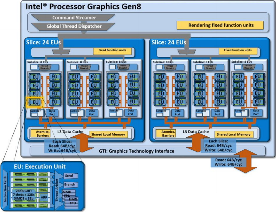
The Intel HD Graphics 6000 (GT3) is an integrated Broadwell graphics card revealed in Q1 2015. It can be found in several ULV SoCs (15 W TDP) such as the Core i5-5250U or i7-5650U. The so-called GT3 GPU offers 48 EUs (Execution Units) and therefore somewhat more shader power than the previous HD 5000 (40 EUs). Depending on the specific CPU, the maximum GPU frequency varies between 950 and 1000 MHz.
Architecture and Features
Broadwell features a GPU based on the Intel Gen8 architecture, which has been optimized in various aspects compared to the previous Gen7.5 (Haswell). Inter alia, the shader arrays called "subslice" have been reorganized and now offer 8 Execution Units (EUs) each. Three subslices form a "slice" for a total of 24 EUs. Combined with other improvements such as larger L1 caches and an optimized frontend, the integrated GPU has become faster and more efficient than its predecessor.
The HD Graphics 6000 represents the top-end version of the Broadwell GPU family and consists of two slices with 48 EUs. Beyond that, there is also a low-end (GT1, 12 EUs), a mid-range (GT2, 24 EUs) and a high-end variant (GT3e, 48 EUs + eDRAM).
All Broadwell GPUs support OpenCL 2.0 and DirectX 12 (FL 11_1). The video engine can now decode H.265 using both fixed function hardware as well as available GPU shaders. Up to three displays can be connected via DP 1.2/eDP 1.3 (max. 3840 x 2160 @ 60 Hz) or HDMI 1.4a (max. 3840 x 2160 @ 24 Hz). HDMI 2.0, however, is not supported.
Performance
Depending on the specific CPU, the maximum GPU frequency varies between 950 and 1000 MHz. Due to the low TDP, however, the average clock in 3D applications will be significantly lower. Overall, the HD Graphics 6000 outperforms the previous HD 5000 by 20 - 25 percent and offers a performance slightly below a dedicated GeForce 820M.
Games as of 2014/2015 will usually run fluently only at (very) low settings.
Power Consumption
Utilizing a new 14 nm process, the Broadwell ULV chips are specified at just 15 W TDP and therefore suited for thin ultrabooks. The TDP is flexible and can be further reduced (9.5 W), which has a significant impact on performance.
Intel Iris Xe Graphics G7 96EUs
► remove from comparisonThe Intel Xe Graphics G7 (Tiger-Lake U GPU with 96 EUs) is a integrated graphics card in the high end Tiger-Lake U CPUs (15 - 28 Watt). It is using the new Xe architecture (Gen12) and was introduced in September 2020. The GPU clocks with a base clock speed (guaranteed) of 400 MHz in all CPUs and can boost up to 1340 MHz (i7-1185G7). The slowest variant offers only 1100 MHz boost (i5-1130G7, 12 Watt TDP).
The performance depends on the TDP settings of the laptop and the used cooling. First informations show that the chip can be configured at 12 and 28 Watt TDP default (as the Ice Lake-U chips) and the performance should be around a dedicated GeForce MX350 in 3DMark benchmarks. For gaming we are expecting a bit worse performance due to the missing dedicated graphics memory and driver support. Many games e.g. had problems when testing the various laptops (e.g. Horizon Zero Dawn or Cyberpunk 2077 did not start or were crashing - see list below). Less demanding games like the Mass Effect Legendary Edition ran in medium settings fine. Compared to the older Ice Lake Iris Plus G7 GPU, the new Tiger Lake GPU should be approximately twice as fast. Therefore, the iGPU is still only for lowest graphical settings and low resolutions in demanding games.
The Tiger Lake SoCs and therefore the integrated GPU are manufactured in the modern 10nm+ (10nm SuperFin) process (improved 10nm process) at Intel and therefore should offer a very good efficiency.
Intel Iris Xe Graphics G7 80EUs
► remove from comparisonThe Intel Xe Graphics G7 80EUs (Tiger-Lake U GPU with 80 EUs) is a integrated graphics card in the mid range Tiger-Lake U CPUs (15 - 28 Watt, e.g. Core i5 11th Gen CPUs). It is using the new Xe architecture (Gen12) and should be announced later in 2020.
The performance depends on the TDP settings of the laptop and the used cooling. First informations show that the chip can be configured at 15 and 28 Watt TDP default (as the Ice Lake-U chips) and the performance should be around a dedicated GeForce MX330 in 3DMark benchmarks. For gaming we are expecting a bit worse performance due to the missing dedicated graphics memory and driver support. Compared to the older Iris Plus G4 in Ice Lake chips, the Tiger Lake GPU should be nearly twice as fast. Benchmarks with various laptops show that the 80EU version lacks about 18% behind the faster 96EU version and on par with the MX330. Compared to AMD iGPUs, the G7 80EU positions itself around the Vega 7 and Vega 8 chips (see chart below for details).
Therefore, the iGPU is still only for lowest graphical settings and low resolutions in demanding games. Some modern games like Days Gone or Cyberpunk wont run over 30 fps in minimum settings (see below).
The Tiger Lake SoCs and therefore the integrated GPU are manufactured in the modern 10nm+ (10nm Superfin) process (improved 10nm process) at Intel and therefore should offer a very good efficiency.
| Intel HD Graphics 6000 | Intel Iris Xe Graphics G7 96EUs | Intel Iris Xe Graphics G7 80EUs | ||||||||||||||||||||||||||||||||||||||||||||||||||||||||||||||||||||||||||||||||||||||||||||||||||||||||||||||||||||||||||||
| Gen. 12 / Xe Series |
|
|
| |||||||||||||||||||||||||||||||||||||||||||||||||||||||||||||||||||||||||||||||||||||||||||||||||||||||||||||||||||||||||||
| Codename | Broadwell GT3 | Tiger Lake Xe | Tiger Lake Xe | |||||||||||||||||||||||||||||||||||||||||||||||||||||||||||||||||||||||||||||||||||||||||||||||||||||||||||||||||||||||||||
| Architecture | Gen. 8 Broadwell | Gen. 11 Ice Lake | Gen. 11 Ice Lake | |||||||||||||||||||||||||||||||||||||||||||||||||||||||||||||||||||||||||||||||||||||||||||||||||||||||||||||||||||||||||||
| Pipelines | 48 - unified | 96 - unified | 80 - unified | |||||||||||||||||||||||||||||||||||||||||||||||||||||||||||||||||||||||||||||||||||||||||||||||||||||||||||||||||||||||||||
| Core Speed | 300 - 1000 (Boost) MHz | 400 - 1350 (Boost) MHz | 400 - 1350 (Boost) MHz | |||||||||||||||||||||||||||||||||||||||||||||||||||||||||||||||||||||||||||||||||||||||||||||||||||||||||||||||||||||||||||
| Memory Bus Width | 64/128 Bit | |||||||||||||||||||||||||||||||||||||||||||||||||||||||||||||||||||||||||||||||||||||||||||||||||||||||||||||||||||||||||||||
| Shared Memory | yes | yes | yes | |||||||||||||||||||||||||||||||||||||||||||||||||||||||||||||||||||||||||||||||||||||||||||||||||||||||||||||||||||||||||||
| API | DirectX 12 (FL 11_1), OpenGL 4.3 | DirectX 12_1, OpenGL 4.6 | DirectX 12_1, OpenGL 4.6 | |||||||||||||||||||||||||||||||||||||||||||||||||||||||||||||||||||||||||||||||||||||||||||||||||||||||||||||||||||||||||||
| Transistors | 1.9 Billion | |||||||||||||||||||||||||||||||||||||||||||||||||||||||||||||||||||||||||||||||||||||||||||||||||||||||||||||||||||||||||||||
| technology | 14 nm | 10 nm | 10 nm | |||||||||||||||||||||||||||||||||||||||||||||||||||||||||||||||||||||||||||||||||||||||||||||||||||||||||||||||||||||||||||
| Features | QuickSync | QuickSync | QuickSync | |||||||||||||||||||||||||||||||||||||||||||||||||||||||||||||||||||||||||||||||||||||||||||||||||||||||||||||||||||||||||||
| Date of Announcement | 05.01.2015 | 15.08.2020 | 15.08.2020 | |||||||||||||||||||||||||||||||||||||||||||||||||||||||||||||||||||||||||||||||||||||||||||||||||||||||||||||||||||||||||||
| Power Consumption | 28 Watt | 28 Watt |
|
|
| ||||||||||||||||||||||||||||||||||||||||||||||||||||||||||||||||||||||||
