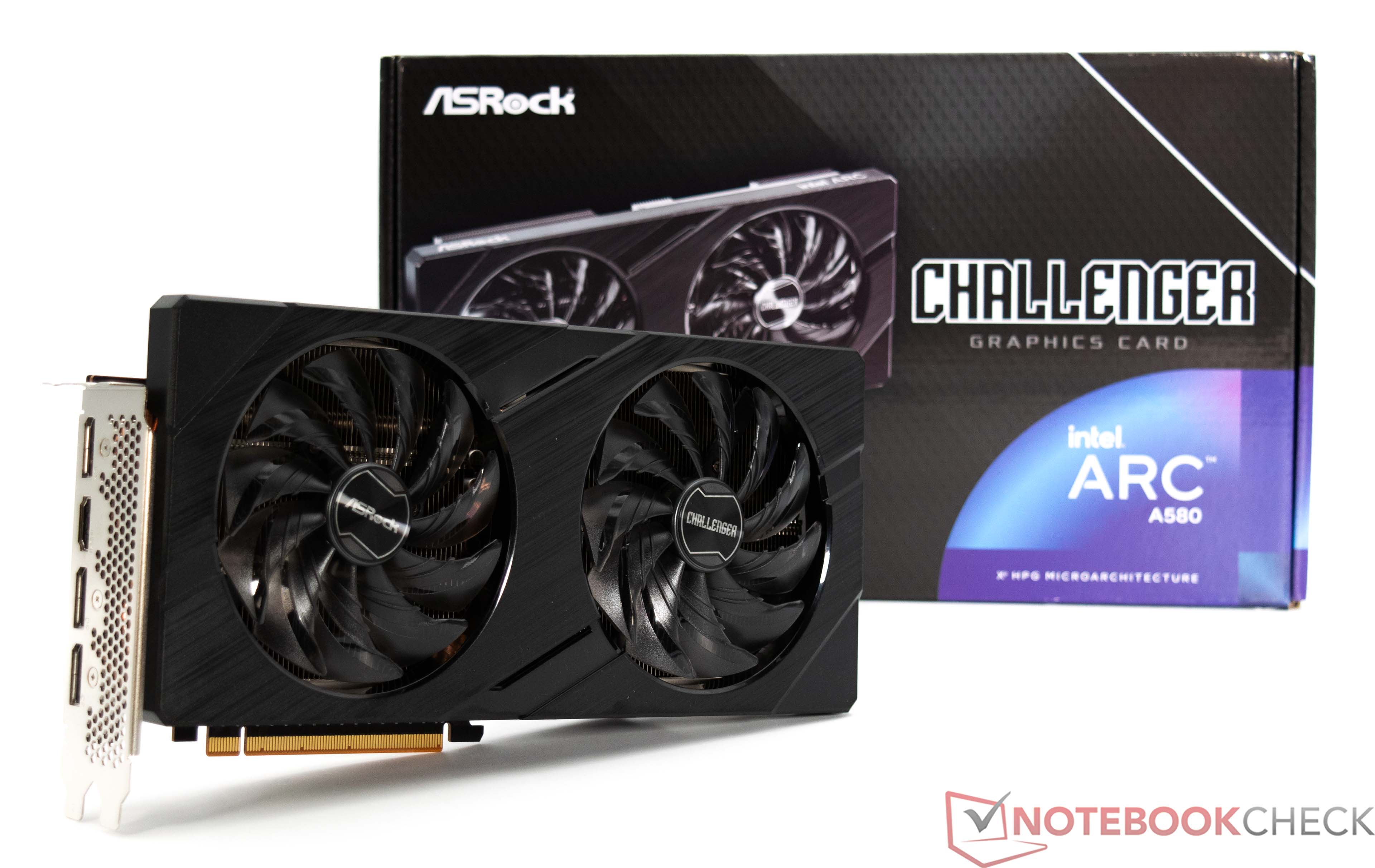
Intel Arc A580

The Intel Arc A580 is an affordable mid-range desktop GPU and is manufactured using the 6 nm process at TSMC. The Intel Arc A580 is also equipped with the DG2-512 graphics chip for the graphics processor, although this only has 3,072 shader units. The VRAM is based on 8 GB GDDR6 with a 256-bit interface (16 Gbps, 512 GB/s). This makes the Intel Arc A580 the third fastest graphics card model from Intel.
Features
Based on the Alchemist architecture, the Intel Arc A580 can rely on the same features as an Intel Arc A750 or an Intel Arc A770. Intel is extremely well positioned in the price range up to 200 euros with the Arc A580. AMD and Nvidia hardly have any suitable models in their portfolios in this price range. Features such as ray tracing are also supported and upscaling technologies such as XeSS can compete with DLSS and FSR. The latter can also be used on Intel graphics cards due to the open standard. With support for AV1, the graphics card is also interesting for content creators. Only the significantly more expensive Ada Lovelace models from Nvidia and the RDNA3 GPUs from AMD are currently capable of hardware-side encoding and decoding with the new codec.
Performance
The performance of the Intel Arc A580 is comparable to an AMD Radeon RX 6600 XT. The Intel Arc A580 can also keep up relatively well with an Intel Arc A750 in the internal duel. Newer games are somewhat more suited to the Intel Arc graphics cards. Nevertheless, many games can now be played well on Intel graphics cards and can be adapted well thanks to the constant driver improvements.
Power consumption
The power consumption of the Intel Arc A580 is estimated by the manufacturer at 175 watts (TGP). In terms of efficiency, however, the Intel Arc A580 is not convincing. Intel is at a disadvantage here compared to AMD and Nvidia. Whether this will change with the successor aka "Battlemage" remains to be seen.
Arc Series
| ||||||||||||||||||||||||||||||||||||||||
Codename | DG2-512 | |||||||||||||||||||||||||||||||||||||||
Architecture | Xe | |||||||||||||||||||||||||||||||||||||||
Pipelines | 3072 - unified | |||||||||||||||||||||||||||||||||||||||
TMUs | 192 | |||||||||||||||||||||||||||||||||||||||
ROPs | 96 | |||||||||||||||||||||||||||||||||||||||
Raytracing Cores | 24 | |||||||||||||||||||||||||||||||||||||||
Tensor / AI Cores | 384 | |||||||||||||||||||||||||||||||||||||||
Core Speed | 1700 - 2000 (Boost) MHz | |||||||||||||||||||||||||||||||||||||||
Theoretical Performance | 24.58 TFLOPS FP16, 12.29 TFLOPS FP32 | |||||||||||||||||||||||||||||||||||||||
Cache | L2: 8 MB | |||||||||||||||||||||||||||||||||||||||
Memory Speed | 16000 effective = 2000 MHz | |||||||||||||||||||||||||||||||||||||||
Memory Bus Width | 256 Bit | |||||||||||||||||||||||||||||||||||||||
Memory Type | GDDR6 | |||||||||||||||||||||||||||||||||||||||
Max. Amount of Memory | 8 GB | |||||||||||||||||||||||||||||||||||||||
Shared Memory | no | |||||||||||||||||||||||||||||||||||||||
Memory Bandwidth | 512 GB/s | |||||||||||||||||||||||||||||||||||||||
API | DirectX 12 Ultimate (12_2), Shader 6.6, OpenGL 4.6, OpenCL 3.0, Vulkan 1.3 | |||||||||||||||||||||||||||||||||||||||
Power Consumption | 175 Watt | |||||||||||||||||||||||||||||||||||||||
Transistor Count | 21.7 Billion | |||||||||||||||||||||||||||||||||||||||
Die Size | 406 mm² | |||||||||||||||||||||||||||||||||||||||
technology | 6 nm | |||||||||||||||||||||||||||||||||||||||
PCIe | 4.0 x16 | |||||||||||||||||||||||||||||||||||||||
Displays | 4 Displays (max.), HDMI 2.1, DisplayPort 2.0 | |||||||||||||||||||||||||||||||||||||||
Date of Announcement | 10.10.2023 |