The Nvidia GeForce RTX 3080 Ti Laptop GPU or 3080 Ti Mobile (for laptops, GN20-E8) is the fastest graphics card for notebooks in early 2022. It is based on the GA103S Ampere chip and offers 7,424 shaders and 16 GB GDDR6 graphics memory with a 256 Bit memory bus. It supports PCIe 4.0 and will be available in different variants (80 - 175 Watt TGP currently known). The maximum Boost clock can vary from 1125 (80 W) to 1590 MHz (150W and up).
There is no more Max-Q variant (formerly used for the low power variants) but every OEM can choose to implement Max-Q technologies (Dynamic Boost, Whispermode).
The performance depends on the TGP setting and cooling of the laptop. Thanks to the higher core count, the RTX 3080 Ti should be clearly faster than the old RTX 3080 Mobile and therefore well suited for 4K gaming.
The GA103S chip offers 7,424 FP32 ALUs of which half can also execute INT32 instructions (i.e. 3,712 INT32 ALUs). With Turing all shaders could still execute FP32 or INT32 instructions. The GA103S integrates 58 Raytracing cores and 232 Tensor cores (e.g., for DLSS). The L2 cache is 4 MB. The Ampere chips also include an improved 5th generation video encoder (NVENC for H.264 and H.265) and a 7th generation decoder (for various formats now including AV1). Compared to the GA103, the GA103S integrates only a 256 Bit memory bus.
The GA103S chip is manufactured by Samsung in 8nm (8N), which is not quite able to keep up with the 7nm node at TSMC (e.g. used by AMD and also for the professional GA100 Ampere chip).
The AMD Radeon RX Vega 2 is an integrated GPU for laptops. It is used for the entry level Athlon Silver 3050U APUs, which were launched in early 2020. The GPU is based on the Vega architecture (5th generation GCN) and has 2 CUs (= 128 of the 704 shaders) clocked at up to 1100 MHz. The performance depends on the configured TDP (12-25 W at launch), the clocks, the cooling, and the memory configuration). The GPU should benefit from fast dual-channel DDR4-2400 RAM (contrary to DDR4-2133 single-channel, which is also possible).
The Vega architecture offers some improvements over the Polaris generation and now supports DirectX 12 Feature Level 12_1. More information is available in our dedicated article about the Raven Ridge architecture.
The performance should be clearly lower than the Radeon RX Vega 3 with 3 CUs and therefore in the lowest performance region of modern GPUs. That means, demanding current games may not be playable fluently.
Thanks to the 12nm process and clever power-saving features, the power consumption is comparatively low (according to AMD), so the graphics card can also be used for slim and light notebooks.
The Nvidia GeForce RTX 3080 Laptop GPU or 3080 Mobile (for laptops, GN20-E7) is the fastest graphics card for notebooks in early 2021. It is based on the GA104-775-A1 Ampere chip and offers 8 or 16 GB GDDR6 graphics memory with a 256 Bit memory bus. It supports PCIe 4.0 and will be available in different variants from 80 - 150 Watt (TGP) (80, 90, 115, 125, 135, 145 and 150+ Watt). As package the notebook graphic card uses GB5-256 and the chip size is 40x40mm. The GPU supports eDP 1.4b to connect the internal monitor.
There is no more Max-Q variant (formerly used for the low power variants) but every OEM can choose to implement Max-Q technologies (Dynamic Boost, Whispermode).
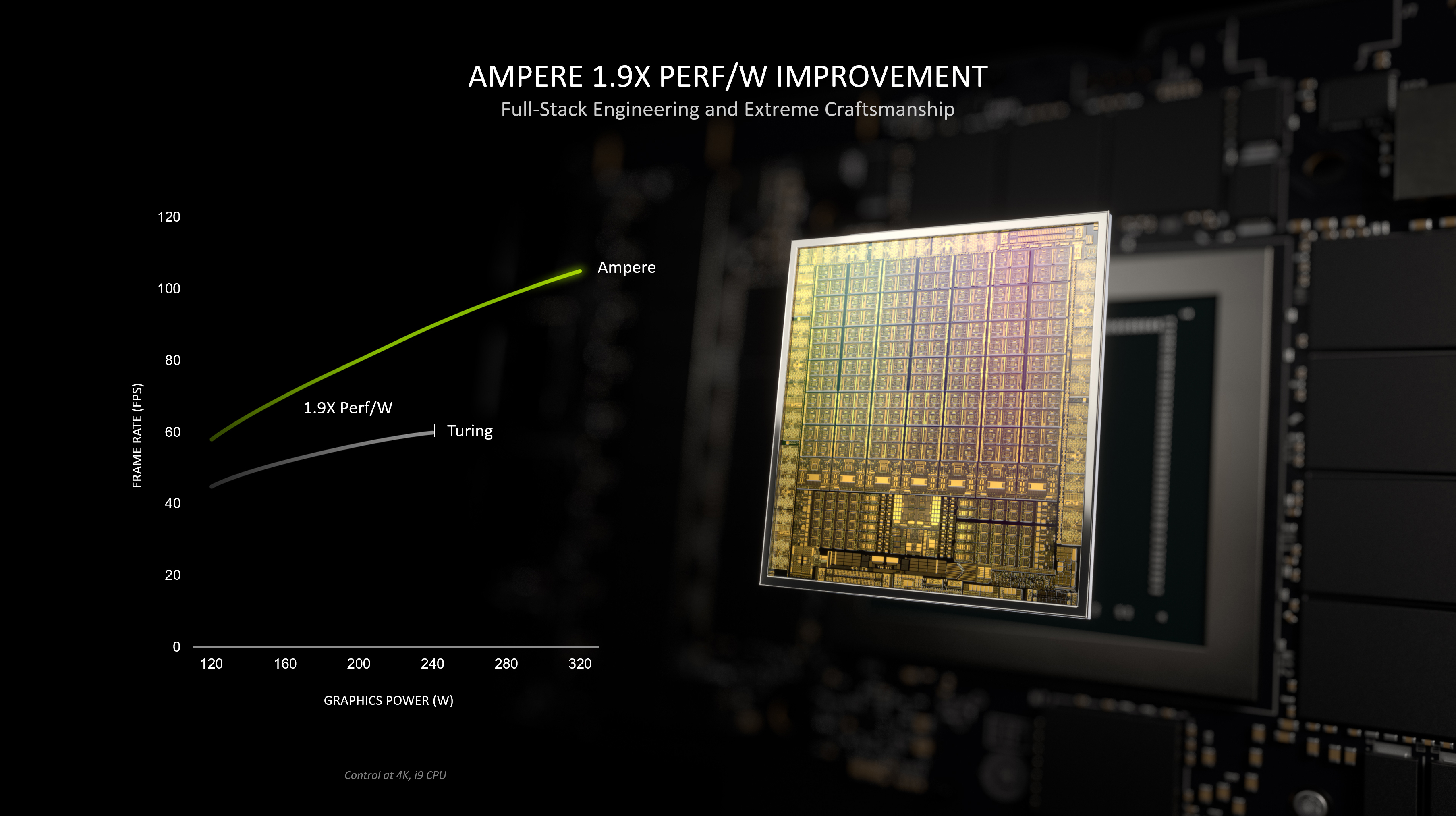
The performance depends on the TGP setting and cooling of the laptop. At the same TGP level the RTX3080 should be faster than the old top model, the RTX 2080 Super Mobile and similar to the desktop RTX 3070. This means, the GPU should be well suited for 4k gaming or QHD with high frame rates. The similar named RTX 3080 desktop card is significantly faster.
The GA104 chip offers 6,144 FP32 ALUs of which half can also execute INT32 instructions (i.e. 3,072 INT32 ALUs). With Turing all shaders could still execute FP32 or INT32 instructions. The raytracing and tensor cores on the chip were also improved according to Nvidia. The Ampere chips also include an improved 5th generation video encoder (NVENC for H.264 and H.265) and a 7th generation decoder (for various formats now including AV1).
The GA104 chip is manufactured by Samsung in 8nm (8N), which is not quite able to keep up with the 7nm node at TSMC (e.g. used by AMD and also for the professional GA100 Ampere chip).