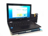
Intel Celeron N4120

The Intel Celeron N4120 is a quad-core SoC primarily for inexpensive notebooks and was announced late 2019. It runs at 1.1-2.6 GHz (Single Core Burst) and is based on the Gemini Lake platform. Compared to the predecessor, the Celeron N4100, the refresh offers a 200 MHz higher Boost clock. Similar to the Apollo Lake predecessors, the chip is manufactured in a 14 nm process with FinFETs but offers slightly improved processor cores, double the amount of L2 cache, a smaller package, a new generation of monitor outputs (Gen 10) and a partly integrated WiFi chip. Besides four CPU cores, the chip also includes a DirectX 12 capable GPU as well as a DDR4/LPDDR4 memory controller (dual-channel, up to 2400 MHz). The SoC is not replaceable as it is directly soldered to the mainboard.
Architecture
The processor architecture ist still called Goldmont Plus. Compared to the older Goldmont cores in Apollo Lake, they feature an increased level 2 cache (to 4 MB). That means the per-clock-performance should be a bit better, but not near the Core CPUs like Kaby Lake Y.
Performance
The CPU performance of the Celeron N4120 is slightly higher than the older N4100 thanks to the 200 MHz higher Boost clock. Compared to the more expensive Core Y processors, especially the single thread performance is much lower in the Gemini Lake based SoCs. Still for basic tasks like office suits, browsing with moderate multitasking the processor performance should be fine.
GPU Performance
The UHD Graphics 600 (Gemini Lake) is based on Intel's Gen9 architecture, which supports DirectX 12 and is also used for the Kaby Lake / Skylake / Apollo Lake graphics adapters (like HD Graphics 520). Equipped with 12 EUs and a clock of up to 700 MHz, the performance should be roughly on par with the older HD Graphics 500 (Apollo Lake).
The chip also includes an advanced video engine with hardware support for the playback of VP9 and H.265 material (8-bit color-depth).
Power Consumption
Similar to the predecessor, Intel specifies the TDP with 6 Watts (SDP 4.8 Watts – Scenario Design Power). The chip can therefore be cooled passively in theory, but SKUs with fans are possible as well.
Series | Intel Gemini Lake | ||||||||||||||||||||||||||||
Codename | Gemini Lake | ||||||||||||||||||||||||||||
Series: Gemini Lake Gemini Lake |
| ||||||||||||||||||||||||||||
Clock Rate | 1100 - 2600 MHz | ||||||||||||||||||||||||||||
Level 2 Cache | 4 MB | ||||||||||||||||||||||||||||
Number of Cores / Threads | 4 / 4 | ||||||||||||||||||||||||||||
Power Consumption (TDP = Thermal Design Power) | 6 Watt | ||||||||||||||||||||||||||||
Manufacturing Technology | 14 nm | ||||||||||||||||||||||||||||
Socket | FCBGA1090 | ||||||||||||||||||||||||||||
Features | Intel UHD Graphics 605 (18 EUs, 200 - 700 MHz), Quick Sync, AES-NI, max. 8 GB Dual-Channel DDR4/LPDDR4-2400 | ||||||||||||||||||||||||||||
GPU | Intel UHD Graphics 600 (200 - 700 MHz) | ||||||||||||||||||||||||||||
64 Bit | 64 Bit support | ||||||||||||||||||||||||||||
Architecture | x86 | ||||||||||||||||||||||||||||
Announcement Date | 11/04/2019 | ||||||||||||||||||||||||||||