

Intel Core i5-8265U vs AMD Ryzen 5 3500U vs AMD Ryzen 5 2600X
Intel Core i5-8265U
► remove from comparisonThe Intel Core i5-8265U is a power efficient quad-core SoC for notebooks and Ultrabooks based on the Whiskey Lake generation and will probably be announced in August 2018. Compared to the similar named Kaby Lake-R processors (e.g. Core i5-8250U), the Whiskey Lake CPUs are now produced in a further improved 14nm process (14nm++) and offer higher clock speeds. The architecture and features are the same. The i5-8265U offers e.g. high Turbo clock speeds of 3,9 GHz (versus 3,4 GHz of the i5-8250U) for a single core (3.8 for two cores, 3.7 GHz for all four cores). The integrated GPU is still named Intel UHD Graphics 620 and the dual-channel memory controller still supports the same RAM speeds as Kaby-Lake-R (DDR4-2400 / LPDDR3-2133). Thermal Velocity Boost is not supported (only in the Core i7-8565U).
The Whiskey Lake SoCs are used with a new PCH produced in 14nm that supports USB 3.1 Gen 2 (10 Gbps) and CNVi WiFi/BT parts.
Architecture
Intel basically uses the same micro architecture compared to Skylake and Kaby Lake, so the per-MHz performance does not differ. That means Whiskey Lake is a Kaby Lake chip manufactured in the improved 14nm++ process.
Performance
The performance of the i5-8265U depends on the cooling solution of the laptop and the defined TDP limits for short and long term performance. We already saw big differences for Kaby Lake-R (e.g., i7-8550U benchmarks), especially for long term (sustained) performance. Therefore, it will be interesting to see how the additionalTurbo clock speed can be made use of. For the Core i7, Intel estimates between 3-11% higher performance to the Kaby-Lake-R generation and that should be similar in the Core i5 (as long as the cooling is sufficient).
Graphics
The integrated Intel UHD Graphics 620 (Intel Gen 9.5) is untouched from the 8th Gen Kaby Lake chips. With fast dual-channel memory it can reach the performance of a dedicated GeForce 920M.
Contrary to Skylake, Kaby Lake and Whiskey Lake now also supports H.265/HEVC Main 10 with a 10-bit color depth as well as Google's VP9 codec. The dual-core Kaby Lake processors announced in January should also support HDCP 2.2.
Power Consumption
The chip is manufactured in a further improved 14nm process with FinFET transistors (14nm++), the same as the 8th Gen Coffee Lake processors. Intel still specifies the TDP with 15 Watts, which is typical for ULV chips. Depending on the usage scenario, the TDP can vary between 7.5 (cTDP Down) and 25 Watts.
Warning: Above information is partly still based on rumors and leaks and may therefore change till release.
AMD Ryzen 5 3500U
► remove from comparisonThe AMD Ryzen 5 3500U is a mobile SoC that was announced in January 2019. It combines four Zen+ cores (8 threads) clocked at 2.1 GHz to 3.7 GHz with a Radeon RX Vega 8 iGPU with 8 CUs (512 Shaders) clocked at up to 1200 MHz. Specified at 15 Watt TDP, the SoC is intended for thin mid-range laptops. In Chromebooks, AMD calles the APU AMD Ryzen 5 3500C, but the specifications (and performance) are the same.
The Picasso SoC uses the Zen+ microarchitecture with slight improvements that should lead to a 3% IPS (performance per clock) improvements. Furthermore, the 12 nm process allows for higher clocks at similar power consumption.
The integrated dual-channel memory controller supports up to DDR4-2400 memory. As the features of the Picasso APUs are the same compared to the Raven Ridge predecessors, we point to our Raven Ridge launch article.
Performance
The average 3500U in our database matches the Intel Core i7-1065G7 in multi-thread performance to be an OK lower mid-range option, as of early 2021.
The Honor MagicBook 14 is among the fastest laptops powered by the 3500U that we know of. It can be up to 50% faster in CPU-bound workloads than the slowest system featuring the same chip in our database, as of August 2023.
Power consumption
This Ryzen 5 series chip has a default TDP (also known as the long-term power limit) of 15 W, a value that laptop makers are free to set to anything between 12 W and 35 W with clock speeds and performance changing accordingly as a result. Either way, this is a tad too high to allow for passively cooled designs.
The chip is manufactured on a 12 nm process for subpar, as of late 2022, energy efficiency.
AMD Ryzen 5 2600X
► remove from comparison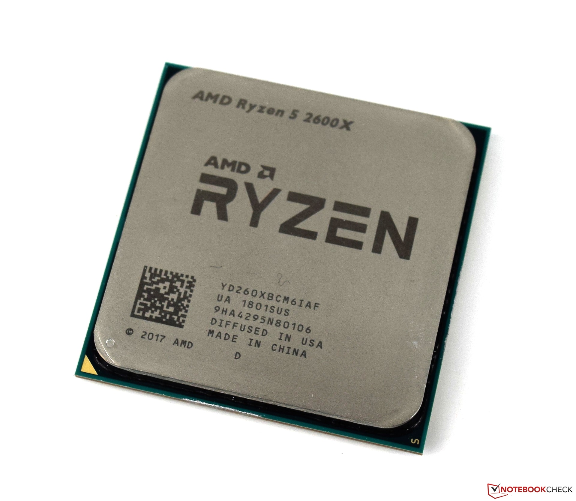
The AMD Ryzen 5 2600X is a high-end desktop processor with 6 cores (12 threads) that was announced early 2018. It is based on the revised Zen+ cores and at launch the second fastest Ryzen CPU behind the Ryzen 7 2700X. The CPU cores clock at 3.6 GHz base and using Precision Boost 2 up to 4.2 GHz. All 6 cores and 12 threads can clock up to 3.9 GHz. The 6 cores are divided in two cluster (3 cores each with own L3 cache) connected via Infinity Fabric.
Compared to the older first Ryzen generation (e.g., Ryzen 5 1600X), the second generation is manufactured in an improved process (12nm called), offers and improved Precision Boost 2 (especially in partial load of the cores) and faster cache and memory speeds.
See our second generation Ryzen review for detailed benchmarks and information.
| Model | Intel Core i5-8265U | AMD Ryzen 5 3500U | AMD Ryzen 5 2600X | ||||||||||||||||||||||||||||||||
| Codename | Whiskey Lake-U | Picasso-U (Zen+) | Zen+ | ||||||||||||||||||||||||||||||||
| Series | Intel Core i5 | AMD Picasso (Ryzen 3000 APU) | AMD Ryzen 5 | ||||||||||||||||||||||||||||||||
| Series: Picasso (Ryzen 3000 APU) Picasso-U (Zen+) |
|
| |||||||||||||||||||||||||||||||||
| Clock | 1600 - 3900 MHz | 2100 - 3700 MHz | 3600 - 4200 MHz | ||||||||||||||||||||||||||||||||
| L1 Cache | 256 KB | 384 KB | |||||||||||||||||||||||||||||||||
| L2 Cache | 1 MB | 2 MB | 4 MB | ||||||||||||||||||||||||||||||||
| L3 Cache | 6 MB | 4 MB | 16 MB | ||||||||||||||||||||||||||||||||
| Cores / Threads | 4 / 8 | 4 / 8 | 6 / 12 | ||||||||||||||||||||||||||||||||
| TDP | 15 Watt | 15 Watt | 95 Watt | ||||||||||||||||||||||||||||||||
| Technology | 14 nm | 12 nm | 12 nm | ||||||||||||||||||||||||||||||||
| Socket | BGA1528 | FP5 | AM4 (1331) | ||||||||||||||||||||||||||||||||
| Features | Dual-Channel DDR4 Memory Controller, HyperThreading, AVX, AVX2, Quick Sync, Virtualization, AES-NI | DDR4-2400 RAM, PCIe 3, MMX, SSE, SSE2, SSE3, SSSE3, SSE4A, SSE4.1, SSE4.2, AVX, AVX2, BMI2, ABM, FMA, ADX, SMEP, SMAP, SMT, CPB, AES-NI, RDRAND, RDSEED, SHA, SME | SSE4.2, SSE4A, AMD-V, AES, AVX2, FMA3, SHA | ||||||||||||||||||||||||||||||||
| iGPU | Intel UHD Graphics 620 (300 - 1100 MHz) | AMD Radeon RX Vega 8 (Ryzen 2000/3000) ( - 1200 MHz) | |||||||||||||||||||||||||||||||||
| Architecture | x86 | x86 | x86 | ||||||||||||||||||||||||||||||||
| Announced | |||||||||||||||||||||||||||||||||||
| Transistors | 4500 Million | 4940 Million | |||||||||||||||||||||||||||||||||
| max. Temp. | 105 °C | ||||||||||||||||||||||||||||||||||
| Manufacturer | www.amd.com | ||||||||||||||||||||||||||||||||||
| Die Size | 209.78 mm2 | ||||||||||||||||||||||||||||||||||
| $229 U.S. |

Benchmarks

Average Benchmarks Intel Core i5-8265U → 100% n=39
Average Benchmarks AMD Ryzen 5 3500U → 93% n=39
Average Benchmarks AMD Ryzen 5 2600X → 162% n=39
* Smaller numbers mean a higher performance
1 This benchmark is not used for the average calculation