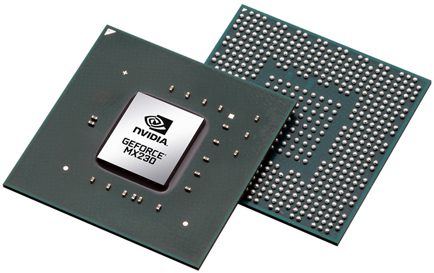
The Nvidia GeForce MX230 is an entry-level dedicated laptop graphics card with DirectX 12 support (FL 12_1) based (most likely) on the Pascal architecture (and not Maxwell as the older MX130). Similar to the faster MX250, the MX230 is based on the GP108 chip.
Features
The GP108 chip is manufactured in a 14 nm FinFET process at Samsung (LPP) and offers a number of new features, including support for DisplayPort 1.4 (ready), HDMI 2.0b, HDR and improved H.265 video de- and encoding (PlayReady 3.0). 4K HDR with Netflix, however, wont run due to the minimum 3 GB graphics memory that is required. Compared to the bigger Pascal chips, the small GP108 does not support Simultaneous Multi-Projection (SMP) for VR and G-Sync. A full list of improvements and the new Pascal desktop GPUs is available in our dedicated Pascal architecture article.
Performance
Thanks to the newer Pascal architecture, the MX230 is significantly faster than the old GeForce MX130 (Maxwell based). Demanding games of 2019 run only in lowest resolution and detail settings and may stutter (e.g. Anno 1800 or Rage 2 ran with under 30fps in our benchmarks). Less demanding games like Overwatch, Fifa 19 or Rocket League, however, can be played in higher detail and resolution settings without stuttering (see benchmarks below).
Power Consumption
The MX230 is manufactured in 14nm at Samsung and due to the low shader count and 64 Bit memory bus, the power consumption is rather low. Therefore, the chip can be also used for small and thin laptops. In our power tests, the faster MX250 needed 22% more power (Furmark load) and the old MX130 even 38% more. The integrated UHD Graphics 620 needed on average only 17% less power at a much lower performance.
The AMD Radeon RX Vega M GH is an integrated GPU in the fastest Intel Kaby-Lake-G SoC. It combines a Kaby-Lake processor, a Vega graphics card and 4 GB HBM2 memory on a single package. The graphics card offers 24 CUs (1536 shaders) and is clocked from 1063 - 1190 MHz.
Currently it looks like the GPU is a mixture of Polaris (Shaders?) and Vega (HBM memory controller at least). E.g. the graphics card is called Polaris 22 internally. Detailed information on the Vega architecture can be found in our dedicated article about the Raven Ridge architecture.
The performance of the Vega M GH should be slightly slower than a dedicated Nvidia GeForce GTX 1060 for laptops according to benchmarks from Intel. Therefore, it should be well suited for 1080p and high resolution gaming.
The power consumption should be quite similar to a dedicated Vega Mobile GPU, but due to the small form factor, smaller laptops can be built with the Kaby-Lake-G SoC. The TDP is specified at 65 Watt for the whole package including GPU, CPU and HBM2 memory.
The AMD Radeon Vega Mobile is a dedicated graphics card for laptops. It most likely uses the same chip as the Kaby-Lake-G graphics part. Rumors currently speak of 28 CUs (= 1792 shaders) instead of the 24 CUs in the Kaby-Lake-G top model. The clock speed should be also around 1 GHz. As graphics memory, the GPU most likely also uses 4 GB HMB2.
The Vega architecture offers some improvements over the Polaris generation and now supports DirectX 12 Feature Level 12_1. More information is available in our dedicated article about the Raven Ridge architecture.
The power consumption should be similar to the Kaby-Lake-G chips (altough this may be more efficient due to power sharing and distribution). The Kaby-Lake-G is rated at 100 Watt including a 35-45 Watt processor.
- Range of benchmark values for this graphics card - Average benchmark values for this graphics card * Smaller numbers mean a higher performance 1 This benchmark is not used for the average calculation
Game Benchmarks
The following benchmarks stem from our benchmarks of review laptops. The performance depends on the used graphics memory, clock rate, processor, system settings, drivers, and operating systems. So the results don't have to be representative for all laptops with this GPU. For detailed information on the benchmark results, click on the fps number.
 Deutsch
 English
 Español
 Français
 Italiano
 Nederlands
 Polski
 Português
 Русский
 Türkçe
 Svenska
 Chinese
 Magyar