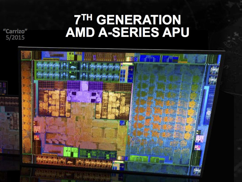
The AMD FX-9830P is a mobile mainstream SoC from the Bristol-Ridge APU series for notebooks (7th APU generation), which was announced mid 2016. The FX-9830P is the fastest Bristol Ridge APU with a 45-Watt TDP and the successor to the 15-35-Watt FX-8800P from the Carrizo generation. The chip has four CPU cores (two Excavator modules = 4 integer and 2 FP units), a Radeon R7 GPU as well as a dual-channel DDR4-1866 memory controller. Carrizo is a full-fledged SoC and is also equipped with an integrated chipset, which provides all I/0 ports.
Architecture
Bristol Ridge is the successor of the Carrizo architecture and the design is almost identical. Thanks to optimized manufacturing processes and more aggressive Boost behavior, however, the clocks are a bit higher at the same power consumption. The memory controller now also supports DDR4-RAM, in this case up to 2400 MHz. More technical details are available in the following articles:
Thanks to higher clocks, the FX9830P is slightly ahead of the old 35-Watt top model FX-8800P and competes with the entry-level dual-cores from Intel (Skylake and Kaby Lake). Compared to the Intel model, the AMD chip has a small advantage in multi-thread scenarios, but is beaten when you only stress one or two cores.
This means there is sufficient performance for typical office and web applications as well as light multitasking.
Graphics Card
The integrated Radeon R7 (Bristol Ridge) GPU has 512 active shader units (8 compute cores) clocked at up to 900 MHz (compared to 758 MHz for FX-9800P). Thanks to the better utilization of the clock range as well as faster DDR4-RAm, the GPU can slightly beat its predecessors Radeon R7 (Carrizo) and competes with a dedicated GeForce 920MX in the best-case scenario (dual-channel memory). Many games from 2015/2016 can be played smoothly at low settings.
Power Consumption
AMD specifies the TDP of the FX-9830P with 25-45 Watts, which is comparable to Intel quad-core processors from the H-series. This means the APU is a good choice for big and heavy notebooks with at least 15 inches.
The Intel Core i5-7360U is a fast dual-core SoC for notebooks and Ultrabooks based on the Kaby Lake architecture and was announced in January 2017. The CPU has two processor cores clocked at 2.3-3.6 GHz (two cores also up to 3.6 GHz). The processor can execute up to four threads simultaneously thanks to Hyper Threading. It is also equipped with an Intel Iris Plus Graphics 640 GPU with 64 MB eDRAM, a dual-channel memory controller (DDR4) as well as VP9 and H.265 video decoding as well as encoding. The chip is still manufactured in a 14nm process with FinFET transistors.
Compared to the Core i7-7560U, the i5-7360 does have lower CPU and GPU clocks.
Architecture
Intel basically uses the same micro architecture compared to Skylake, so the per-MHz performance does not differ. The manufacturer only reworked the Speed Shift technology for faster dynamic adjustments of voltages and clocks, and the improved 14nm process allows much higher frequencies combined with better efficiency than before.
Performance
At 2.3-3.6 GHz, the Core i5-7360U has a slightly lower base frequency but higher Turbo clocks compared to the Core i5-7300U and is therefore faster. The CPU part can also use the 64 MB eDRAM, which should increase the performance in some scenarios.
Graphics
The integrated Intel Iris Plus 640 Graphics is the GT3e model of the Kaby Lake GPU (Intel Gen. 9.5). It has 48 Execution Units running at 300-1000 MHz (i7 models up to 1050 MHz) and the performance is comparable to a GeForce 920MX thanks to fast eDRAM cache. However, there aren't any significant improvements compared to the old Iris Pro 540, so modern games can often not be played smoothly or only at the lowest or medium settings, respectively.
Contrary to Skylake, Kaby lake now also supports H.265/HEVC Main 10 with a 10-bit color depth as well as Google's VP9 codec. The dual-core Kaby Lake processors announced in January should also support HDCP 2.2.
Power Consumption
The chip is manufactured in an improved 14nm process with FinFET transistors, which improves the efficiency even further. Intel still specifies the TDP with 15 Watts, which is typical for ULV chips. Depending on the usage scenario, the TDP can vary between 7.5 (cTDP Down) and 25 Watts.
The Intel Core i7-7500U is a dual-core processor of the Kaby Lake architecture. It offers two CPU cores clocked at 2.7 - 3.5 GHz and integrates HyperThreading to work with up to 4 threads at once. The architectural differences are rather small compared to the Skylake generation, therefore the performance per MHz is very similar. The SoC includes a dual channel DDR4 memory controller and Intel HD Graphics 620 graphics card (clocked at 300 - 1050 MHz). It is manufactured in an improved 14nm FinFET process (14nm+) at Intel. Compared to the old Skylake Core i7-6500U (2.5 - 3.1 GHz), the i7-7500U clock speed is up to 400 MHz higher.
- Range of benchmark values for this graphics card - Average benchmark values for this graphics card * Smaller numbers mean a higher performance 1 This benchmark is not used for the average calculation
v1.26
log 19. 16:54:12
#0 checking url part for id 8165 +0s ... 0s
#1 checking url part for id 8449 +0s ... 0s
#2 checking url part for id 8149 +0s ... 0s
#3 not redirecting to Ajax server +0s ... 0s
#4 did not recreate cache, as it is less than 5 days old! Created at Sun, 19 May 2024 05:35:32 +0200 +0.001s ... 0.001s
#5 composed specs +0.038s ... 0.039s
#6 did output specs +0s ... 0.039s
#7 getting avg benchmarks for device 8165 +0.003s ... 0.042s
#8 got single benchmarks 8165 +0.011s ... 0.053s
#9 getting avg benchmarks for device 8449 +0.003s ... 0.056s
#10 got single benchmarks 8449 +0.01s ... 0.065s
#11 getting avg benchmarks for device 8149 +0.004s ... 0.069s
#12 got single benchmarks 8149 +0.255s ... 0.324s
#13 got avg benchmarks for devices +0s ... 0.324s
#14 min, max, avg, median took s +0.331s ... 0.655s
 Deutsch
 English
 Español
 Français
 Italiano
 Nederlands
 Polski
 Português
 Русский
 Türkçe
 Svenska
 Chinese
 Magyar