 Deutsch
 English
 Español
 Français
 Italiano
 Nederlands
 Polski
 Português
 Русский
 Türkçe
 Svenska
 Chinese
 Magyar
Intel Core i7-6500U vs AMD Ryzen 5 2600 vs Intel Core i7-6650U
Intel Core i7-6500U
► remove from comparison
The Intel Core i7-6500U is an ULV (ultra low voltage) dual-core SoC based on the Skylake architecture and has been launched in September 2015. The CPU can be found in ultrabooks as well as normal notebooks. In addition to two CPU cores with Hyper-Threading clocked at 2.5 - 3.1 GHz (2 cores: max. 3.0 GHz), the chip also integrates an HD Graphics 520 GPU and a dual-channel DDR4-2133/DDR3L-1600 memory controller. The SoC is manufactured using a 14 nm process with FinFET transistors.
Architecture
Skylake replaces both Haswell and Broadwell and brings the same microarchitecture in every TDP class from 4.5 to 45 W. The extensive improvements of the Skylake design include increased out-of-order buffers, optimized prefetching and branch prediction as well as additional performance gains through Hyper-Threading. Overall, however, performance per clock has been increased by only 5 to 10 percent (compared to Haswell) respectively under 5 percent (compard to Broadwell), which is quite modest for a new architecture ("Tock").
Performance
According to the specified clock rates and the improved architecture, the Core i7-6500U should perform similar to a Core i5-4300M (Haswell, 37 W) or a Core i7-5600U (Broadwell, 15 W). Thus, the CPU has sufficient power for office and multimedia purposes as well as more demanding applications and multitasking.
Graphics
The integrated graphics unit called HD Graphics 520 represents the "GT2" version of the Skylake GPU (Intel Gen. 9). The 24 Execution Units, also called EUs, are clocked at 300 - 1050 MHz and offer a performance somewhere in range of a dedicated GeForce 820M. Games of 2015 can thus be played smoothly in low settings. For more information about performance and features, check our page for the HD Graphics 520.
Power Consumption
Specified at a TDP of 15 W (including CPU, GPU and memory controller), the CPU is best suited for small notebooks and ultrabooks (11-inches and above). Optionally, the TDP can be lowered to 7.5 watts (cTDP down), reducing both heat dissipation and performance and allowing even more compact designs.
AMD Ryzen 5 2600
► remove from comparison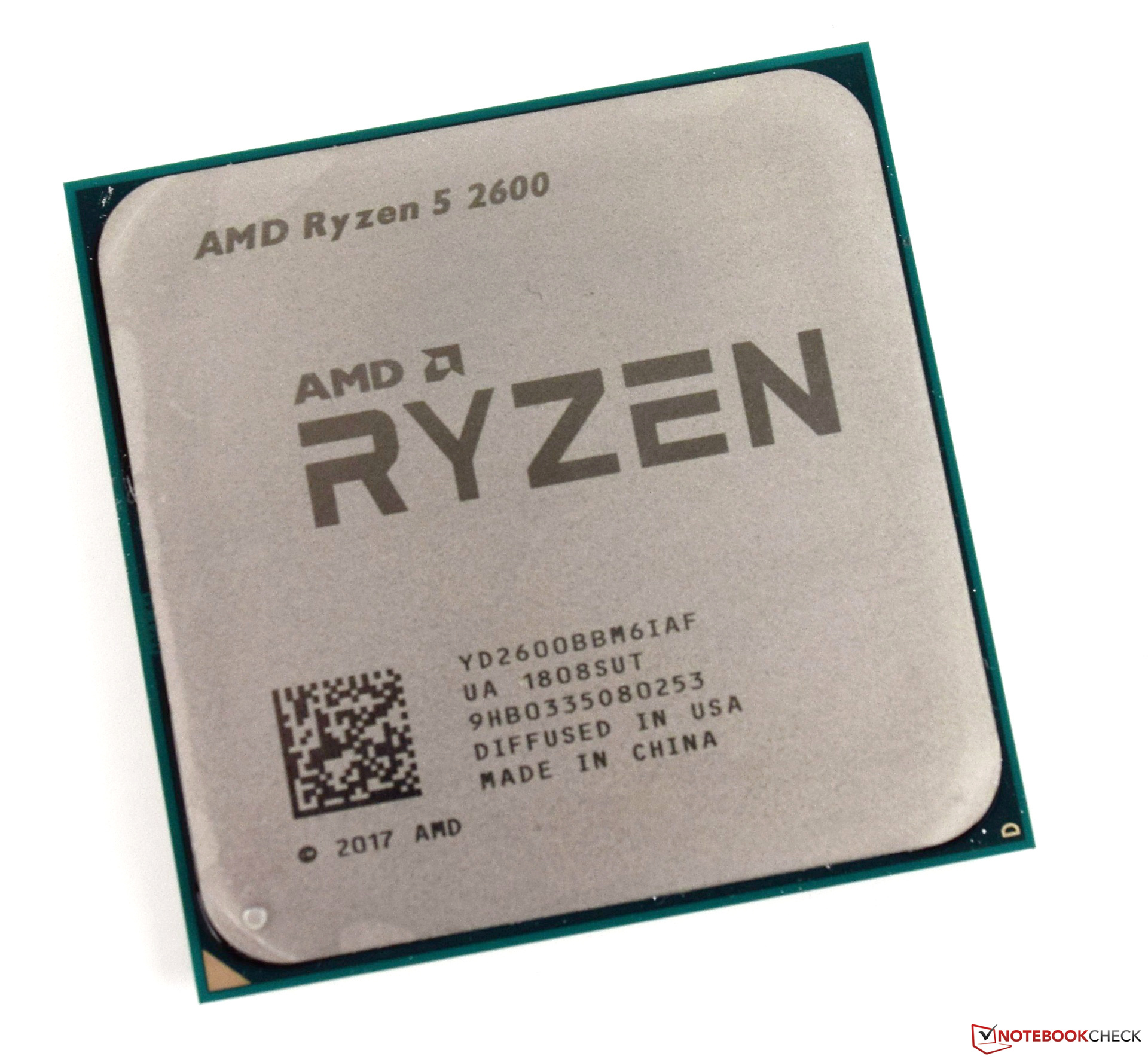
The AMD Ryzen 5 2600 is a six-core desktop processor that can handle twelve threads simultaneously thanks to Simultaneous Multithreading (SMT). This technology is equivalent to Intel's Hyper-Threading. Launched in April 2018, the Ryzen 5 2600 is the second fastest Ryzen 5 processor and is much more economical than its flagship sibling. The Ryzen 5 2600 has a 65 W TDP, which is nearly 40% more efficient than the 95 W TDP Ryzen 5 2600 X. This energy efficiency comes at a cost to performance though.
The Ryzen 5 2600 has a base clock speed of 3.4 GHz, which can be boosted by Extended Frequency Range (XFR) up to 3.9 GHz. The power gain is still high in multi-threaded applications, although this is some way off the Ryzen 5 2600X. The Ryzen 5 2600 benefits from AMD's new Zen+ architecture, with a greater number of instructions per cycle (IPC) and higher clock speeds than last year's Zen chips. The Ryzen 5 2600's six cores are divided into two clusters that are connected by Infinity Fabric, a subset of HyperTransport. Each cluster has its own L3 cache.
The Ryzen 5 2600 has good performance in games. Moreover, the Ryzen 5 2600 has a higher base clock than the Ryzen 7 2700. Seeing as many games currently lack multi-core support, this means that the Ryzen 5 2600 performs better than its technically superior sibling.
Detailed information, benchmarks and values can be found in our review of the Ryzen 5 2600.
Intel Core i7-6650U
► remove from comparison
The Intel Core i7-6650U is an ULV (ultra low voltage) dual-core SoC based on the Skylake architecture. In September 2015, it's the fastest CPU of the 15 W series (besides the i7-6600U) and can be found in ultrabooks as well as normal notebooks. In addition to two CPU cores with Hyper-Threading clocked at 2.2 - 3.4 GHz (2 cores: max. 3.2 GHz), the chip also integrates an Iris Graphics 540 GPU with 64 MB of dedicated eDRAM memory and a dual-channel DDR4-2133/DDR3L-1600 memory controller. The SoC is manufactured using a 14 nm process with FinFET transistors.
Architecture
Skylake replaces both Haswell and Broadwell and brings the same microarchitecture in every TDP class from 4.5 to 45 W. The extensive improvements of the Skylake design include increased out-of-order buffers, optimized prefetching and branch prediction as well as additional performance gains through Hyper-Threading. Overall, however, performance per clock has been increased by only 5 to 10 percent (compared to Haswell) respectively under 5 percent (compard to Broadwell), which is quite modest for a new architecture ("Tock").
Furthermore, the organisation of the eDRAM cache has been modified. Instead of acting like a victim cache, which has to be adressed via the L3/LLC, the eDRAM can now be adressed directly by programms just like the main memory. The size is still 128 MB for the quad-core models (4C + GT4e), while the dual-core chips (2C + GT3e) only offer 64 MB.
Performance
According to the specified clock rates and the improved architecture, the Core i7-6650U should perform similar to a Core i5-4310M (Haswell, 37 W) and is one of the fastest ULV dual-cores as of late 2015. Thus, the CPU has sufficient power for office and multimedia purposes as well as more demanding applications and multitasking.
Graphics
The integrated graphics unit called Iris Graphics 540 represents the "GT3e" version of the Skylake GPU (Intel Gen. 9). The 48 Execution Units, also called EUs, are clocked at 300 - 1050 MHz and offer (thanks to the fast eDRAM cache) a performance sligthly above a dedicated GeForce 920M. Games of 2015 can thus be played smoothly in low or medium settings. For more information about performance and features, check our page for the Iris Graphics 540.
Power Consumption
Specified at a TDP of 15 W (including CPU, GPU and memory controller), the CPU is best suited for small notebooks and ultrabooks (11-inches and above). Optionally, the TDP can be lowered to 9.5 watts (cTDP down), reducing both heat dissipation and performance and allowing even more compact designs.
| Model | Intel Core i7-6500U | AMD Ryzen 5 2600 | Intel Core i7-6650U | ||||||||||||||||||||||||||||||||||||||||||||||||||||||||||||||||||||||||||||||||||||||||||||||||
| Series | Intel Core i7 | AMD Ryzen 5 | Intel Core i7 | ||||||||||||||||||||||||||||||||||||||||||||||||||||||||||||||||||||||||||||||||||||||||||||||||
| Codename | Skylake | Pinnacle Riege (Zen+) | Skylake | ||||||||||||||||||||||||||||||||||||||||||||||||||||||||||||||||||||||||||||||||||||||||||||||||
| Series: Core i7 Skylake |
|
| |||||||||||||||||||||||||||||||||||||||||||||||||||||||||||||||||||||||||||||||||||||||||||||||||
| Clock | 2500 - 3100 MHz | 3400 - 3900 MHz | 2200 - 3400 MHz | ||||||||||||||||||||||||||||||||||||||||||||||||||||||||||||||||||||||||||||||||||||||||||||||||
| L1 Cache | 128 KB | 128 KB | |||||||||||||||||||||||||||||||||||||||||||||||||||||||||||||||||||||||||||||||||||||||||||||||||
| L2 Cache | 512 KB | 3 MB | 512 KB | ||||||||||||||||||||||||||||||||||||||||||||||||||||||||||||||||||||||||||||||||||||||||||||||||
| L3 Cache | 4 MB | 16 MB | 4 MB | ||||||||||||||||||||||||||||||||||||||||||||||||||||||||||||||||||||||||||||||||||||||||||||||||
| Cores / Threads | 2 / 4 | 6 / 12 | 2 / 4 | ||||||||||||||||||||||||||||||||||||||||||||||||||||||||||||||||||||||||||||||||||||||||||||||||
| TDP | 15 Watt | 65 Watt | 15 Watt | ||||||||||||||||||||||||||||||||||||||||||||||||||||||||||||||||||||||||||||||||||||||||||||||||
| Technology | 14 nm | 12 nm | 14 nm | ||||||||||||||||||||||||||||||||||||||||||||||||||||||||||||||||||||||||||||||||||||||||||||||||
| Die Size | 99 mm2 | 213 mm2 | |||||||||||||||||||||||||||||||||||||||||||||||||||||||||||||||||||||||||||||||||||||||||||||||||
| max. Temp. | 100 °C | 95 °C | 100 °C | ||||||||||||||||||||||||||||||||||||||||||||||||||||||||||||||||||||||||||||||||||||||||||||||||
| Socket | BGA | AM4 (LGA1331) | BGA | ||||||||||||||||||||||||||||||||||||||||||||||||||||||||||||||||||||||||||||||||||||||||||||||||
| Features | Dual-Channel DDR3L-1600/DDR4-2133 Memory Controller, HyperThreading, AVX, AVX2, Quick Sync, Virtualization, AES-NI | DDR4-2933 RAM, PCIe 3, MMX, SSE, SSE2, SSE3, SSSE3, SSE4A, SSE4.1, SSE4.2, AVX, AVX2, BMI2, ABM, FMA, ADX, SMEP, SMAP, SMT, CPB, AES-NI, RDRAND, RDSEED, SHA, SME | Dual-Channel DDR3L-1600/DDR4-2133 Memory Controller, HyperThreading, AVX, AVX2, Quick Sync, Virtualization, AES-NI, vPro, TXT | ||||||||||||||||||||||||||||||||||||||||||||||||||||||||||||||||||||||||||||||||||||||||||||||||
| iGPU | Intel HD Graphics 520 (300 - 1050 MHz) | Intel Iris Graphics 540 (300 - 1050 MHz) | |||||||||||||||||||||||||||||||||||||||||||||||||||||||||||||||||||||||||||||||||||||||||||||||||
| Architecture | x86 | x86 | |||||||||||||||||||||||||||||||||||||||||||||||||||||||||||||||||||||||||||||||||||||||||||||||||
| $393 U.S. | $415 U.S. | ||||||||||||||||||||||||||||||||||||||||||||||||||||||||||||||||||||||||||||||||||||||||||||||||||
| Announced | |||||||||||||||||||||||||||||||||||||||||||||||||||||||||||||||||||||||||||||||||||||||||||||||||||
| Manufacturer | ark.intel.com | www.amd.com | ark.intel.com | ||||||||||||||||||||||||||||||||||||||||||||||||||||||||||||||||||||||||||||||||||||||||||||||||
| Transistors | 4940 Million |

