 Deutsch
 English
 Español
 Français
 Italiano
 Nederlands
 Polski
 Português
 Русский
 Türkçe
 Svenska
 Chinese
 Magyar
Intel HD Graphics P630 vs NVIDIA GeForce MX230
Intel HD Graphics P630
► remove from comparison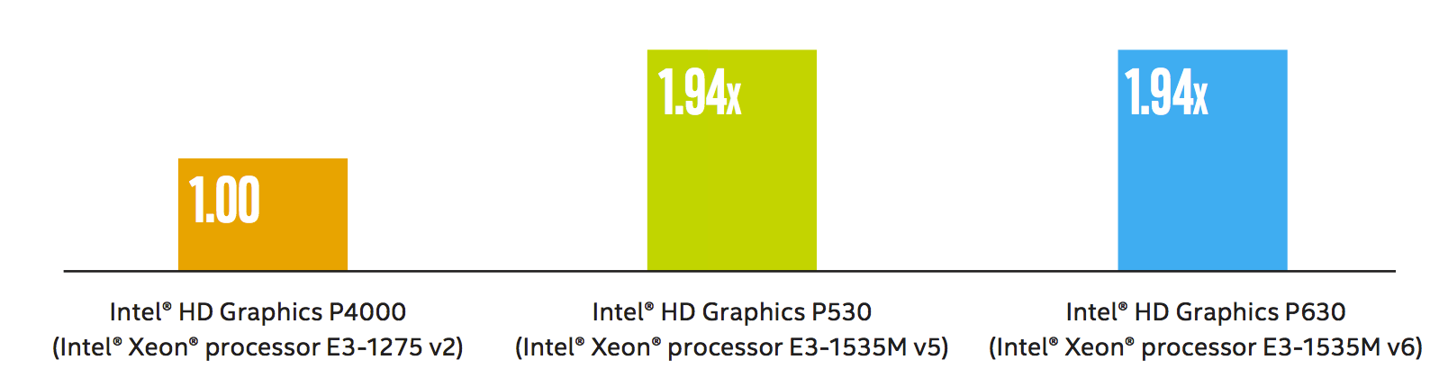
The Intel HD Graphics P630 (GT2) is an integrated graphics unit, which can be found in various Xeon workstation processors of the Kaby Lake generation. The "GT2" version of the Skylake GPU offers 24 Execution Units (EUs) clocked at up to 1050 MHz (depending on the CPU model). Due to its lack of dedicated graphics memory or eDRAM cache, the P630 has to access the main memory (2x 64bit DDR3L-1600 / DDR4-2133). It uses the same silicon as the consumer HD Graphics 630 in Kaby-Lake-H processors but features optimized drivers for workstaion and CAD software. According to Intel it is certified for 15 applications (see list).
Performance
According to Intel, the performance of the P630 is identical to the Intel HD Graphis P530 (Skylake predecessor) processor graphics card and 1.94x faster than the old Intel HD Graphics P4000. Compared to consumer cards, the gaming performance should be on a similar level to the dedicated GeForce 920M and will handle old games (as of 2015) in low or medium settings.
Features
The revised video engine in the Kaby Lake chips now supports H.265/HEVC Main10 profile at 10-bit color depth and also the VP9 codec in hardware. Furthermore, HDCP 2.2 is also supported in all chips, which allows Netflix 4K videos, for instance.
Power Consumption
The HD Graphics P630 can be found in mobile quad-core Xeon processors with 45 W TDP and also desktop processors of the Xeon range with higher TDPs.
Source: http://www.intel.com/content/dam/www/public/us/en/documents/guides/hd-graphics-performance-guide.pdf
NVIDIA GeForce MX230
► remove from comparison
The Nvidia GeForce MX230 is an entry-level dedicated laptop graphics card with DirectX 12 support (FL 12_1) based (most likely) on the Pascal architecture (and not Maxwell as the older MX130). Similar to the faster MX250, the MX230 is based on the GP108 chip.
Features
The GP108 chip is manufactured in a 14 nm FinFET process at Samsung (LPP) and offers a number of new features, including support for DisplayPort 1.4 (ready), HDMI 2.0b, HDR and improved H.265 video de- and encoding (PlayReady 3.0). 4K HDR with Netflix, however, wont run due to the minimum 3 GB graphics memory that is required. Compared to the bigger Pascal chips, the small GP108 does not support Simultaneous Multi-Projection (SMP) for VR and G-Sync. A full list of improvements and the new Pascal desktop GPUs is available in our dedicated Pascal architecture article.
Performance
Thanks to the newer Pascal architecture, the MX230 is significantly faster than the old GeForce MX130 (Maxwell based). Demanding games of 2019 run only in lowest resolution and detail settings and may stutter (e.g. Anno 1800 or Rage 2 ran with under 30fps in our benchmarks). Less demanding games like Overwatch, Fifa 19 or Rocket League, however, can be played in higher detail and resolution settings without stuttering (see benchmarks below).
Power Consumption
The MX230 is manufactured in 14nm at Samsung and due to the low shader count and 64 Bit memory bus, the power consumption is rather low. Therefore, the chip can be also used for small and thin laptops. In our power tests, the faster MX250 needed 22% more power (Furmark load) and the old MX130 even 38% more. The integrated UHD Graphics 620 needed on average only 17% less power at a much lower performance.
| Intel HD Graphics P630 | NVIDIA GeForce MX230 | ||||||||||||||||||||||||||||||||||||||||||||||
| GeForce MX200 Series |
|
| |||||||||||||||||||||||||||||||||||||||||||||
| Codename | Kaby-Lake-H-GT2 | N17S-G0 | |||||||||||||||||||||||||||||||||||||||||||||
| Architecture | Gen. 9.5 Kaby Lake | Pascal | |||||||||||||||||||||||||||||||||||||||||||||
| Pipelines | 24 - unified | 256 - unified | |||||||||||||||||||||||||||||||||||||||||||||
| Memory Bus Width | 64/128 Bit | 64 Bit | |||||||||||||||||||||||||||||||||||||||||||||
| Shared Memory | yes | no | |||||||||||||||||||||||||||||||||||||||||||||
| API | DirectX 12_1, OpenGL 4.4 | DirectX 12_1, Shader 5.0, OpenGL 4.5 | |||||||||||||||||||||||||||||||||||||||||||||
| technology | 14 nm | 14 nm | |||||||||||||||||||||||||||||||||||||||||||||
| Features | QuickSync | Vulcan 1.1, GPU Boost 3.0, Optimus, PhysX, CUDA, GeForce Experience, GameWorks | |||||||||||||||||||||||||||||||||||||||||||||
| Date of Announcement | 05.08.2015 | 20.02.2019 | |||||||||||||||||||||||||||||||||||||||||||||
| Core Speed | 1519 - 1531 (Boost) MHz | ||||||||||||||||||||||||||||||||||||||||||||||
| Memory Speed | 7000 MHz | ||||||||||||||||||||||||||||||||||||||||||||||
| Memory Type | GDDR5 | ||||||||||||||||||||||||||||||||||||||||||||||
| Max. Amount of Memory | 4 GB | ||||||||||||||||||||||||||||||||||||||||||||||
| Transistors | 1.8 Billion | ||||||||||||||||||||||||||||||||||||||||||||||
| Notebook Size | medium sized | ||||||||||||||||||||||||||||||||||||||||||||||
| Link to Manufacturer Page | www.geforce.com |
| |||||||||||||||||


