

Intel Core i7-1255U vs AMD Ryzen 9 3900X vs AMD Ryzen 3 3100
Intel Core i7-1255U
► remove from comparisonThe Intel Core i7-1255U is a high-end mobile CPU for thin and light laptops based on the Alder Lake architecture. It was announced in early 2022 and offers 2 performance cores (P-cores, Golden Cove architecture) and 8 efficient cores (E-cores, Gracemont architecture). The P-cores support Hyper-Threading leading to 12 supported threads when combined with the E-cores. The clock rate ranges from 1.7 to 4.7 GHz on the performance cluster and 1.2 to 3.5 GHz on the efficient cluster. The performance of the E-cores should be similar to old Skylake cores (compare to the Core i7-6700HQ). All cores can use up to 12 MB L3 cache. Compared to the i7-1265U (fastest U-series CPU at launch), the 1255 offers 100 MHz lower clocked CPU cores and only "Essentials" vPro management features. Compared to the P-series (28W) or H-series (45W), the 15W TDP may limit the sustained performance.
Performance
The average 1255U in our database is in the same league as the Ryzen 5 5600U, as far as multi-thread benchmark scores are concerned. Which is nothing to be ashamed of, as of mid 2023.
Thanks to its decent cooling solution and a long-term CPU power limit of 28 W, the Spectre x360 13.5 14t-ef000 is among the fastest laptops built around the 1255U that we know of. It can be 20% faster in CPU-bound workloads than the slowest system featuring the same chip in our database, as of August 2023.
Architecture
The integrated memory controller supports various memory types up to DDR5-4800, DDR4-3200, LPDDR5-5200, and LPDDR4x-4267. The Thread Director (in hardware) can support the operating system to decide which thread to use on the performance or efficient cores for the best performance. For AI tasks, the CPU also integrates GNA 3.0 and DL Boost (via AVX2). Quick Sync in version 8 is the same as in the Rocket Lake CPUs and supports MPEG-2, AVC, VC-1 decode, JPEG, VP8 decode, VP9, HEVC, and AV1 decode in hardware. The CPU only supports PCIe 4.0 (x8 for a GPU and two x4 for SSDs).
The integrated graphics card is based on the Xe-architecture and offers all 96 EUs (Execution Units) operating at up to 1.25 GHz.
Power consumption
This Core i7 has a "minimum assured" power consumption of 12 W. Its Base power consumption sits at 15 W and its maximum Intel-recommended Turbo power consumption isn't supposed to exceed 55 W. All those values are too high to allow for pasisvely cooled designs.
Last but not the least, Core i7-1255U is built with Intel's fourth-gen 10 nm process marketed as Intel 7 for decent, as of late 2022, energy efficiency.
AMD Ryzen 9 3900X
► remove from comparison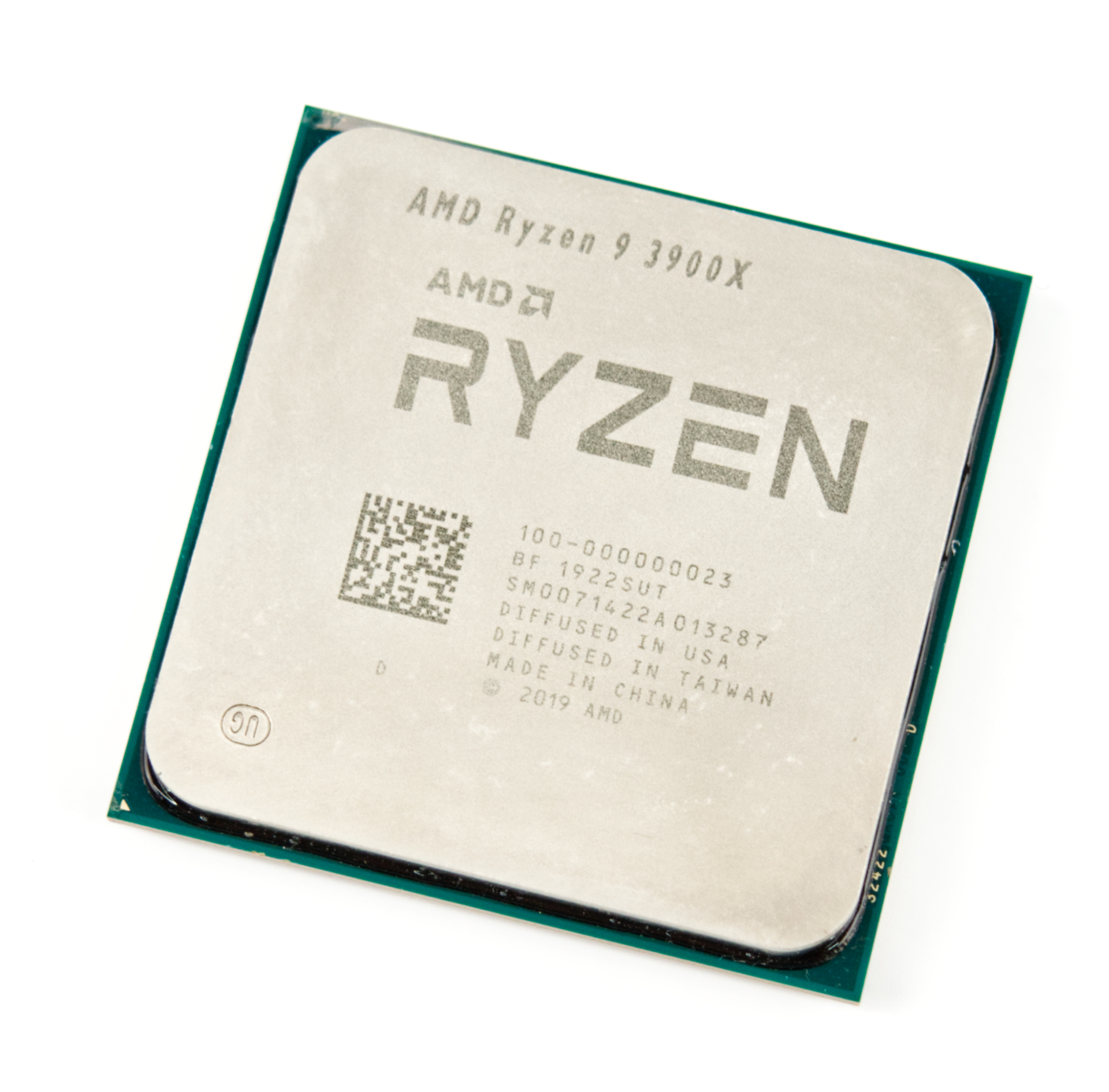
Der AMD Ryzen 9 3900X ist ein Desktop-Prozessor der Matisse Serie mit 12-Kernen und Hyperthreading (SMT), weshalb dieser 24 Threads gleichzeitig verarbeiten kann. Mit dem Launch am 07.07.2019 ist der Ryzen 9 3900X der schnellste Ryzen 9 Prozessor und mit 105 Watt TDP spezifiziert. Bis zur endgültigen Verfügbarkeit des Ryzen 9 3950X bleibt der Ryzen 9 3900X allerdings das Topmodell, denn der Ryzen 9 3950X soll erst im September 2019 folgen und insgesamt 16 Kerne bieten.
Der Ryzen 9 3900X taktet mit 3,8 GHz Basistakt und kann per Turbo auf bis zu 4,6 GHz takten. Bei Last aller 12 Kerne erreicht der Ryzen 9 3900X maximal 4,3 GHz. Dank des Precision Boost 2 kann der Takt auf einem höheren Level gehalten werden, wie wir es schon von Zen+ her kennen.
Die Leistung des AMD Ryzen 9 3900X ist durchweg bei allen Anwendungen hervorragend. Vor allem bei Multi-Thread-Anwendungen kann hier der native 12-Kerner seine Stärken ausspielen und kann es sogar mit einem AMD Threadripper 1950X aufnehmen.
Die vier CCX-Cluster bestehend aus jeweils 4 CPU-Kernen, von denen jeweils drei aktiv sind befinden sich in zwei CCD-Packages (je 3 Kerne mit eigenem 16 MByte L3 Cache). Ein CCD-Package ist genau 74 mm² groß und wird im neuen 7 nm Verfahren bei TSMC gefertigt. Bei den beiden Ryzen-9-Prozessoren befinden sich zwei dieser CCD-Einheiten unter dem Heatspreader. Der I/O-Die ist separiert und kommt im mit der älteren 12 nm Strukturbreite daher, welcher weiterhin von Gobalfoundries gefertigt.
Bei Spielen kann der AMD Ryzen 9 3900X dank der verbesserten IPC überzeugen. Schlussendlich kommt es jedoch immer auf die Unterstützung der Spiele an. Wer nur Spielen möchte, ist gut beraten sich den AMD Ryzen 7 3700X genauer anzuschauen. Wer jedoch gleichzeitig Streamen oder Videos bearbeiten möchte, für diejenigen ist der Ryzen 9 3900X die bessere Wahl.
AMD Ryzen 3 3100
► remove from comparison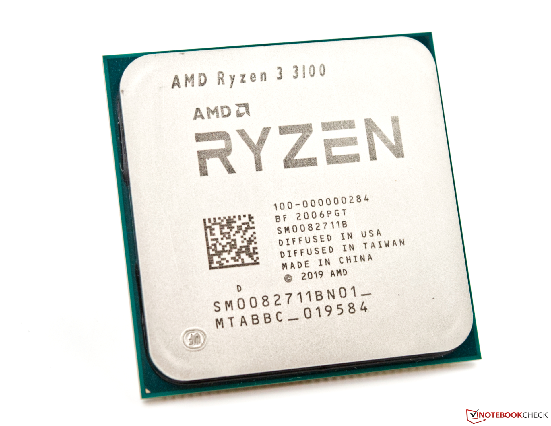
The Ryzen 3 3100 is a cheap entry level desktop processor of the Matisse series with 4 cores and 8 threads. It clocks from 3.6 (base) - 3.9 GHz (boost) and uses the Zen 2 microarchitecture. It uses two CCX clusters with two cores each. Therefore, there are some disadvantages compared to the faster Ryzen 3 3300X that uses all four cores of a single CCX-cluster. The CPU is manufactured on the modern 7 nm process at TSMC. The I/O die that is not part of the main die is manufactured on 12 nm at Globalfoundries. The TDP is 65 Watts and therefore the CPU won't need a big beefy cooler.
In multi-threaded applications the performance of the Ryzen 3 3100 can reach the old Core i7-7700K (a former high end CPU). In games and single threaded applications, the performance is slightly lower as the higher clocked Ryzen 3 3300X is on par with the 7700K. Still, the 3100 can be a good pick for an entry level gaming system.
| Model | Intel Core i7-1255U | AMD Ryzen 9 3900X | AMD Ryzen 3 3100 | ||||||||||||||||||||||||||||||||||||||||||||||||||||||||||||||||||||||||||||||||||||||||||||||||||||||||||||||||
| Codename | Alder Lake-U | Matisse (Zen 2) | Matisse (Zen 2) | ||||||||||||||||||||||||||||||||||||||||||||||||||||||||||||||||||||||||||||||||||||||||||||||||||||||||||||||||
| Series | Intel Alder Lake-M | AMD Matisse (Ryzen 3000 Desktop) | AMD Matisse (Ryzen 3000 Desktop) | ||||||||||||||||||||||||||||||||||||||||||||||||||||||||||||||||||||||||||||||||||||||||||||||||||||||||||||||||
| Series: Matisse (Ryzen 3000 Desktop) Matisse (Zen 2) |
|
|
| ||||||||||||||||||||||||||||||||||||||||||||||||||||||||||||||||||||||||||||||||||||||||||||||||||||||||||||||||
| Clock | 1200 - 4700 MHz | 3800 - 4600 MHz | 3600 - 3900 MHz | ||||||||||||||||||||||||||||||||||||||||||||||||||||||||||||||||||||||||||||||||||||||||||||||||||||||||||||||||
| L1 Cache | 928 KB | 768 KB | 256 KB | ||||||||||||||||||||||||||||||||||||||||||||||||||||||||||||||||||||||||||||||||||||||||||||||||||||||||||||||||
| L2 Cache | 9.5 MB | 6 MB | 2 MB | ||||||||||||||||||||||||||||||||||||||||||||||||||||||||||||||||||||||||||||||||||||||||||||||||||||||||||||||||
| L3 Cache | 12 MB | 64 MB | 16 MB | ||||||||||||||||||||||||||||||||||||||||||||||||||||||||||||||||||||||||||||||||||||||||||||||||||||||||||||||||
| Cores / Threads | 10 / 12 | 12 / 24 | 4 / 8 | ||||||||||||||||||||||||||||||||||||||||||||||||||||||||||||||||||||||||||||||||||||||||||||||||||||||||||||||||
| TDP | 15 Watt | 105 Watt | 65 Watt | ||||||||||||||||||||||||||||||||||||||||||||||||||||||||||||||||||||||||||||||||||||||||||||||||||||||||||||||||
| Technology | 10 nm | 7 nm | 7 nm | ||||||||||||||||||||||||||||||||||||||||||||||||||||||||||||||||||||||||||||||||||||||||||||||||||||||||||||||||
| max. Temp. | 100 °C | 95 °C | |||||||||||||||||||||||||||||||||||||||||||||||||||||||||||||||||||||||||||||||||||||||||||||||||||||||||||||||||
| Socket | BGA1744 | AM4 (LGA1331) | AM4 (LGA1331) | ||||||||||||||||||||||||||||||||||||||||||||||||||||||||||||||||||||||||||||||||||||||||||||||||||||||||||||||||
| Features | DDR4-3200/LPDDR4x-4266/DDR5-4800/LPDDR5-5200 RAM, PCIe 4, Thr. Dir., DL Boost, GNA, vPro Ess., MMX, SSE, SSE2, SSE3, SSSE3, SSE4.1, SSE4.2, AVX, AVX2, BMI2, ABM, FMA, ADX, SMEP, SMAP, EIST, TM1, TM2, HT, Turbo, SST, AES-NI, RDRAND, RDSEED, SHA | DDR4-3200 RAM, PCIe 4, MMX, SSE, SSE2, SSE3, SSSE3, SSE4A, SSE4.1, SSE4.2, AVX, AVX2, BMI2, ABM, FMA, ADX, SMEP, SMAP, SMT, CPB, AES-NI, RDRAND, RDSEED, SHA, SME | DDR4-3200 RAM, PCIe 4, MMX, SSE, SSE2, SSE3, SSSE3, SSE4A, SSE4.1, SSE4.2, AVX, AVX2, BMI2, ABM, FMA, ADX, SMEP, SMAP, SMT, CPB, AES-NI, RDRAND, RDSEED, SHA, SME | ||||||||||||||||||||||||||||||||||||||||||||||||||||||||||||||||||||||||||||||||||||||||||||||||||||||||||||||||
| iGPU | Intel Iris Xe Graphics G7 96EUs ( - 1250 MHz) | ||||||||||||||||||||||||||||||||||||||||||||||||||||||||||||||||||||||||||||||||||||||||||||||||||||||||||||||||||
| Architecture | x86 | x86 | x86 | ||||||||||||||||||||||||||||||||||||||||||||||||||||||||||||||||||||||||||||||||||||||||||||||||||||||||||||||||
| Announced | |||||||||||||||||||||||||||||||||||||||||||||||||||||||||||||||||||||||||||||||||||||||||||||||||||||||||||||||||||
| Manufacturer | ark.intel.com | www.amd.com | www.amd.com | ||||||||||||||||||||||||||||||||||||||||||||||||||||||||||||||||||||||||||||||||||||||||||||||||||||||||||||||||
| $499 U.S. | $99 U.S. |

Benchmarks

Average Benchmarks Intel Core i7-1255U → 100% n=20
Average Benchmarks AMD Ryzen 9 3900X → 145% n=20
Average Benchmarks AMD Ryzen 3 3100 → 78% n=20
* Smaller numbers mean a higher performance
1 This benchmark is not used for the average calculation