Deutsch
 English
 Español
 Français
 Italiano
 Nederlands
 Polski
 Português
 Русский
 Türkçe
 Svenska
 Chinese
 Magyar
AMD Radeon RX Vega M GH vs AMD Radeon RX Vega 2 vs AMD Radeon RX Vega Mobile
AMD Radeon RX Vega M GH
► remove from comparison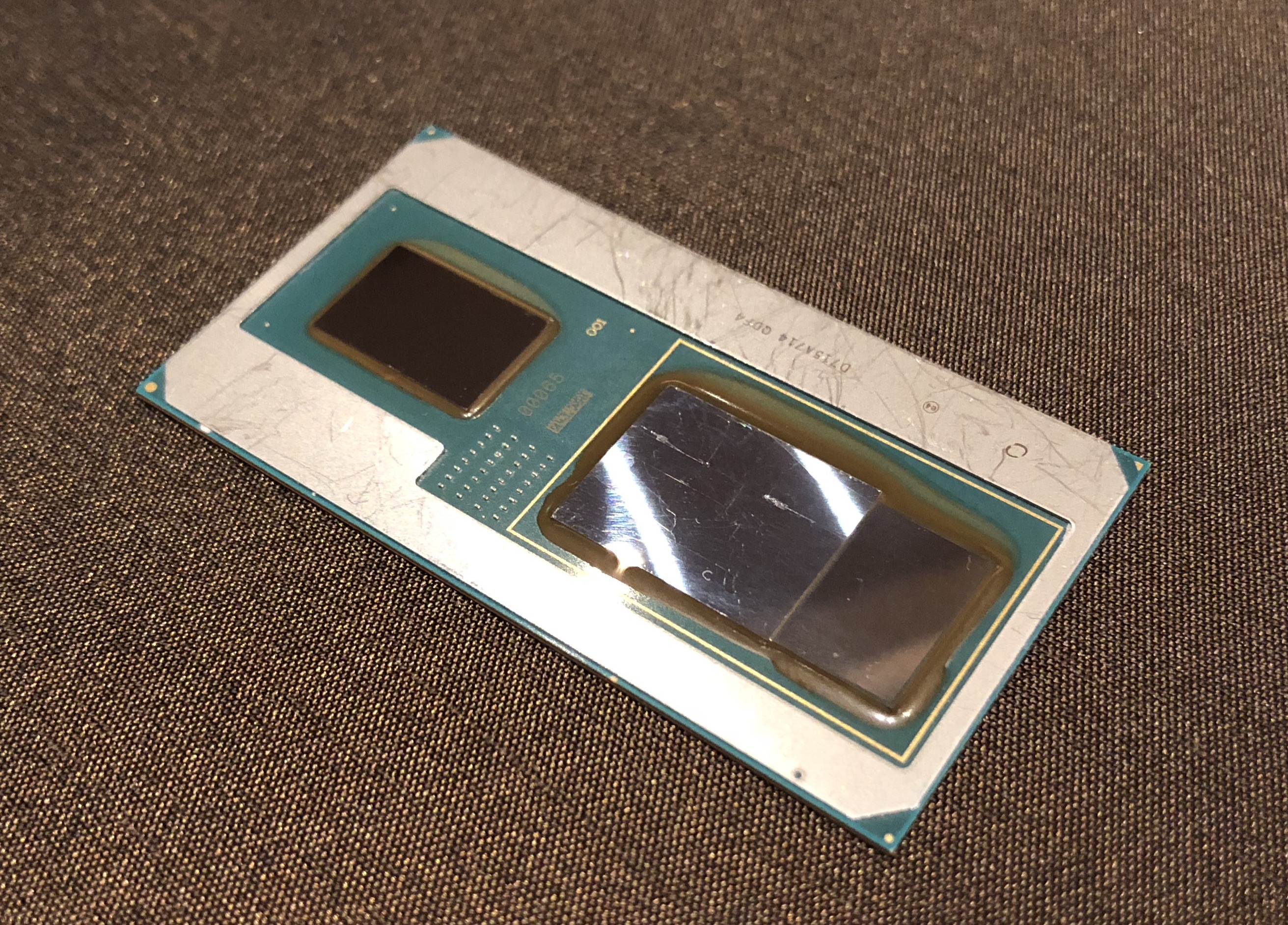
The AMD Radeon RX Vega M GH is an integrated GPU in the fastest Intel Kaby-Lake-G SoC. It combines a Kaby-Lake processor, a Vega graphics card and 4 GB HBM2 memory on a single package. The graphics card offers 24 CUs (1536 shaders) and is clocked from 1063 - 1190 MHz.
Currently it looks like the GPU is a mixture of Polaris (Shaders?) and Vega (HBM memory controller at least). E.g. the graphics card is called Polaris 22 internally. Detailed information on the Vega architecture can be found in our dedicated article about the Raven Ridge architecture.
The performance of the Vega M GH should be slightly slower than a dedicated Nvidia GeForce GTX 1060 for laptops according to benchmarks from Intel. Therefore, it should be well suited for 1080p and high resolution gaming.
The power consumption should be quite similar to a dedicated Vega Mobile GPU, but due to the small form factor, smaller laptops can be built with the Kaby-Lake-G SoC. The TDP is specified at 65 Watt for the whole package including GPU, CPU and HBM2 memory.
AMD Radeon RX Vega 2
► remove from comparison
The AMD Radeon RX Vega 2 is an integrated GPU for laptops. It is used for the entry level Athlon Silver 3050U APUs, which were launched in early 2020. The GPU is based on the Vega architecture (5th generation GCN) and has 2 CUs (= 128 of the 704 shaders) clocked at up to 1100 MHz. The performance depends on the configured TDP (12-25 W at launch), the clocks, the cooling, and the memory configuration). The GPU should benefit from fast dual-channel DDR4-2400 RAM (contrary to DDR4-2133 single-channel, which is also possible).
The Vega architecture offers some improvements over the Polaris generation and now supports DirectX 12 Feature Level 12_1. More information is available in our dedicated article about the Raven Ridge architecture.
The performance should be clearly lower than the Radeon RX Vega 3 with 3 CUs and therefore in the lowest performance region of modern GPUs. That means, demanding current games may not be playable fluently.
Thanks to the 12nm process and clever power-saving features, the power consumption is comparatively low (according to AMD), so the graphics card can also be used for slim and light notebooks.
AMD Radeon RX Vega Mobile
► remove from comparison
The AMD Radeon Vega Mobile is a dedicated graphics card for laptops. It most likely uses the same chip as the Kaby-Lake-G graphics part. Rumors currently speak of 28 CUs (= 1792 shaders) instead of the 24 CUs in the Kaby-Lake-G top model. The clock speed should be also around 1 GHz. As graphics memory, the GPU most likely also uses 4 GB HMB2.
The Vega architecture offers some improvements over the Polaris generation and now supports DirectX 12 Feature Level 12_1. More information is available in our dedicated article about the Raven Ridge architecture.
The power consumption should be similar to the Kaby-Lake-G chips (altough this may be more efficient due to power sharing and distribution). The Kaby-Lake-G is rated at 100 Watt including a 35-45 Watt processor.
The Radeon Vega Mobile was announced one day before CES at a press event by Lisa Su.
| AMD Radeon RX Vega M GH | AMD Radeon RX Vega 2 | AMD Radeon RX Vega Mobile | |||||||||||||||||||||||||||||||||||||||||||||||||||||||||||||
| AMD Radeon RX Vega Series |
|
|
| ||||||||||||||||||||||||||||||||||||||||||||||||||||||||||||
| Codename | Vega Kaby Lake-G | Vega Raven Ridge | Vega Mobile | ||||||||||||||||||||||||||||||||||||||||||||||||||||||||||||
| Architecture | Vega | Vega | Vega | ||||||||||||||||||||||||||||||||||||||||||||||||||||||||||||
| Pipelines | 1536 - unified | 128 - unified | 1792 - unified | ||||||||||||||||||||||||||||||||||||||||||||||||||||||||||||
| Core Speed | 1063 - 1190 (Boost) MHz | 1100 (Boost) MHz | |||||||||||||||||||||||||||||||||||||||||||||||||||||||||||||
| Memory Type | HBM2 | HBM2 | |||||||||||||||||||||||||||||||||||||||||||||||||||||||||||||
| Max. Amount of Memory | 4 GB | 4 GB | |||||||||||||||||||||||||||||||||||||||||||||||||||||||||||||
| Shared Memory | no | no | no | ||||||||||||||||||||||||||||||||||||||||||||||||||||||||||||
| API | DirectX 12_1 | DirectX 12_1 | DirectX 12_1 | ||||||||||||||||||||||||||||||||||||||||||||||||||||||||||||
| Power Consumption | 100 Watt | 15 Watt | 90 Watt | ||||||||||||||||||||||||||||||||||||||||||||||||||||||||||||
| technology | 14 nm | 12 nm | 14 nm | ||||||||||||||||||||||||||||||||||||||||||||||||||||||||||||
| Features | Tiled Rasterization, Shared Memory (up to Dual-Channel DDR4-2400) | Tiled Rasterization, Shared Memory (up to Dual-Channel DDR4-2400) | |||||||||||||||||||||||||||||||||||||||||||||||||||||||||||||
| Notebook Size | medium sized | medium sized | |||||||||||||||||||||||||||||||||||||||||||||||||||||||||||||
| Date of Announcement | 07.01.2018 | 07.01.2018 | 07.01.2018 | ||||||||||||||||||||||||||||||||||||||||||||||||||||||||||||
| Transistors | 4.5 Billion | ||||||||||||||||||||||||||||||||||||||||||||||||||||||||||||||
| Memory Bus Width | 2048 Bit |
|
| |||||||||||||||||||||||||