 Deutsch
 English
 Español
 Français
 Italiano
 Nederlands
 Polski
 Português
 Русский
 Türkçe
 Svenska
 Chinese
 Magyar
Intel Core i7-6650U vs AMD A12-9700P vs Intel Core i7-6820HK
Intel Core i7-6650U
► remove from comparison
The Intel Core i7-6650U is an ULV (ultra low voltage) dual-core SoC based on the Skylake architecture. In September 2015, it's the fastest CPU of the 15 W series (besides the i7-6600U) and can be found in ultrabooks as well as normal notebooks. In addition to two CPU cores with Hyper-Threading clocked at 2.2 - 3.4 GHz (2 cores: max. 3.2 GHz), the chip also integrates an Iris Graphics 540 GPU with 64 MB of dedicated eDRAM memory and a dual-channel DDR4-2133/DDR3L-1600 memory controller. The SoC is manufactured using a 14 nm process with FinFET transistors.
Architecture
Skylake replaces both Haswell and Broadwell and brings the same microarchitecture in every TDP class from 4.5 to 45 W. The extensive improvements of the Skylake design include increased out-of-order buffers, optimized prefetching and branch prediction as well as additional performance gains through Hyper-Threading. Overall, however, performance per clock has been increased by only 5 to 10 percent (compared to Haswell) respectively under 5 percent (compard to Broadwell), which is quite modest for a new architecture ("Tock").
Furthermore, the organisation of the eDRAM cache has been modified. Instead of acting like a victim cache, which has to be adressed via the L3/LLC, the eDRAM can now be adressed directly by programms just like the main memory. The size is still 128 MB for the quad-core models (4C + GT4e), while the dual-core chips (2C + GT3e) only offer 64 MB.
Performance
According to the specified clock rates and the improved architecture, the Core i7-6650U should perform similar to a Core i5-4310M (Haswell, 37 W) and is one of the fastest ULV dual-cores as of late 2015. Thus, the CPU has sufficient power for office and multimedia purposes as well as more demanding applications and multitasking.
Graphics
The integrated graphics unit called Iris Graphics 540 represents the "GT3e" version of the Skylake GPU (Intel Gen. 9). The 48 Execution Units, also called EUs, are clocked at 300 - 1050 MHz and offer (thanks to the fast eDRAM cache) a performance sligthly above a dedicated GeForce 920M. Games of 2015 can thus be played smoothly in low or medium settings. For more information about performance and features, check our page for the Iris Graphics 540.
Power Consumption
Specified at a TDP of 15 W (including CPU, GPU and memory controller), the CPU is best suited for small notebooks and ultrabooks (11-inches and above). Optionally, the TDP can be lowered to 9.5 watts (cTDP down), reducing both heat dissipation and performance and allowing even more compact designs.
AMD A12-9700P
► remove from comparison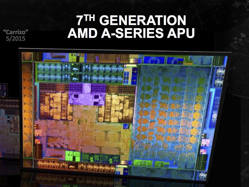
The AMD A12-9700P is a mainstream SoC from the Bristol-Ridge APU series for notebooks (7th APU generation), which was announced mid 2016. The ULV chip with a TDP of 15 Watts (can be configured to 12 Watts) has four CPU cores (two Excavator modules), a Radeon R7 GPU as well as a dual-channel DDR4-1866 memory controller. Carrizo is a full-fledged SoC and is also equipped with an integrated chipset, which provides all I/0 ports.
Architecture
Bristol Ridge is the successor of the Carrizo architecture and the design is almost identical. Thanks to optimized manufacturing processes and more aggressive Boost behavior, however, the clocks are a bit higher at the same power consumption. The memory controller now also supports DDR4-RAM, in this case up to 1866 MHz. More technical details are available in the following articles:
Performance
The performance of the A12-9700P is between the two 15-Watt processors A10-9600P and FX-9800P, and therefore roughly on par with a 15-Watt Core i3 from the Skylake or Kaby Lake series, respectively. Compared to the Intel model, the AMD chip has a small advantage in multi-thread scenarios, but is beaten when you only stress one or two cores. Due to the TDP limitation, the performance of the A12-9700P will drop significantly under sustained workloads.
This means there is sufficient performance for typical office and web applications as well as light multitasking.
Graphics Card
The integrated Radeon R7 (Bristol Ridge) GPU has 512 active shader units (8 compute cores) clocked at up to 758 MHz. Thanks to the better utilization of the clock range as well as faster DDR4-RAm, the GPU can slightly beat its predecessors Radeon R7 (Carrizo) and competes with a dedicated GeForce 920MX in the best-case scenario (dual-channel memory, low CPU requirements). Many games from 2015/2016 can be played smoothly at low settings.
Power Consumption
AMD specifies the TDP of the A12-9700P with 15 Watts, which is comparable to Intel's ULV models. This means the CPU is a good choice for thin notebooks starting with a 12-inch screen.
Intel Core i7-6820HK
► remove from comparison
The Intel Core i7-6820HK is a quad-core processor based on the Skylake architecture, that has been launched in September 2015. In addition to four CPU cores with Hyper-Threading clocked at 2.7 - 3.6 GHz (4 cores: max. 3.2 GHz, 2 cores: max. 3.4 GHz), the chip also integrates an HD Graphics 530 GPU and a dual-channel DDR4-2133/DDR3L-1600 memory controller. The CPU is manufactured using a 14 nm process with FinFET transistors.
Currently, the i7-6820HK is the only Skylake chip with an unlocked multiplier for easy overclocking (similar to previous Extreme Editions).
Architecture
Skylake replaces both Haswell and Broadwell and brings the same microarchitecture in every TDP class from 4.5 to 45 W. The extensive improvements of the Skylake design include increased out-of-order buffers, optimized prefetching and branch prediction as well as additional performance gains through Hyper-Threading. Overall, however, performance per clock has been increased by only 5 to 10 percent (compared to Haswell) respectively under 5 percent (compard to Broadwell), which is quite modest for a new architecture ("Tock").
Performance
Tanks to the improved architecture, the Core i7-6820HK performs roughly on par with the former Core i7-4900MQ (Haswell) or the Core i7-5700HQ (Broadwell). Under long-lasting full load, the Skylake chip will take the lead over most of its Haswell-based predecessors, as the advanced 14 nm process leads to a higher energy efficiency and reduces throttling. If the 6820HK is overclocked (we've tested up to 4.0 GHz on all 4 cores), the performance will be even better.
Even the most demanding applications and excessive multitasking are handled easily.
Graphics
The integrated graphics unit called HD Graphics 530 represents the "GT2" version of the Skylake GPU (Intel Gen. 9). The 24 Execution Units, also called EUs, are clocked at 350 - 1050 MHz and offer a performance about 20 percent above the old HD Graphics 4600. Games of 2015 can thus be played smoothly in low or medium settings. For more information about performance and features, check our page for the HD Graphics 530.
Power Consumption
Specified at a TDP of 45 W (including CPU, GPU and memory controller), the CPU is best suited for bigger notebooks 15-inches in size and above. Optionally, the TDP can be lowered to 35 watts (cTDP down), reducing both heat dissipation and performance.
| Model | Intel Core i7-6650U | AMD A12-9700P | Intel Core i7-6820HK | ||||||||||||||||||||||||||||||||||||||||||||||||||||||||||||||||||||||||||||||||||||||||||||||||||||||||||||||||||||||||||||||||||||
| Series | Intel Core i7 | AMD Bristol Ridge | Intel Core i7 | ||||||||||||||||||||||||||||||||||||||||||||||||||||||||||||||||||||||||||||||||||||||||||||||||||||||||||||||||||||||||||||||||||||
| Codename | Skylake | Bristol Ridge | Skylake | ||||||||||||||||||||||||||||||||||||||||||||||||||||||||||||||||||||||||||||||||||||||||||||||||||||||||||||||||||||||||||||||||||||
| Series: Core i7 Skylake |
|
|
| ||||||||||||||||||||||||||||||||||||||||||||||||||||||||||||||||||||||||||||||||||||||||||||||||||||||||||||||||||||||||||||||||||||
| Clock | 2200 - 3400 MHz | 2500 - 3400 MHz | 2700 - 3600 MHz | ||||||||||||||||||||||||||||||||||||||||||||||||||||||||||||||||||||||||||||||||||||||||||||||||||||||||||||||||||||||||||||||||||||
| L1 Cache | 128 KB | 256 KB | |||||||||||||||||||||||||||||||||||||||||||||||||||||||||||||||||||||||||||||||||||||||||||||||||||||||||||||||||||||||||||||||||||||
| L2 Cache | 512 KB | 2 MB | 1 MB | ||||||||||||||||||||||||||||||||||||||||||||||||||||||||||||||||||||||||||||||||||||||||||||||||||||||||||||||||||||||||||||||||||||
| L3 Cache | 4 MB | 8 MB | |||||||||||||||||||||||||||||||||||||||||||||||||||||||||||||||||||||||||||||||||||||||||||||||||||||||||||||||||||||||||||||||||||||
| Cores / Threads | 2 / 4 | 4 / 4 | 4 / 8 | ||||||||||||||||||||||||||||||||||||||||||||||||||||||||||||||||||||||||||||||||||||||||||||||||||||||||||||||||||||||||||||||||||||
| TDP | 15 Watt | 15 Watt | 45 Watt | ||||||||||||||||||||||||||||||||||||||||||||||||||||||||||||||||||||||||||||||||||||||||||||||||||||||||||||||||||||||||||||||||||||
| Technology | 14 nm | 28 nm | 14 nm | ||||||||||||||||||||||||||||||||||||||||||||||||||||||||||||||||||||||||||||||||||||||||||||||||||||||||||||||||||||||||||||||||||||
| max. Temp. | 100 °C | 90 °C | 100 °C | ||||||||||||||||||||||||||||||||||||||||||||||||||||||||||||||||||||||||||||||||||||||||||||||||||||||||||||||||||||||||||||||||||||
| Socket | BGA | FP4 | BGA | ||||||||||||||||||||||||||||||||||||||||||||||||||||||||||||||||||||||||||||||||||||||||||||||||||||||||||||||||||||||||||||||||||||
| Features | Dual-Channel DDR3L-1600/DDR4-2133 Memory Controller, HyperThreading, AVX, AVX2, Quick Sync, Virtualization, AES-NI, vPro, TXT | Dual-Channel DDR3/DDR4-1866 Memory Controller, PCIe 3.0 x8 | Dual-Channel DDR3L-1600/DDR4-2133 Memory Controller, AVX, AVX2, Quick Sync, Virtualization, AES-NI | ||||||||||||||||||||||||||||||||||||||||||||||||||||||||||||||||||||||||||||||||||||||||||||||||||||||||||||||||||||||||||||||||||||
| iGPU | Intel Iris Graphics 540 (300 - 1050 MHz) | AMD Radeon R7 (Bristol Ridge) ( - 758 MHz) | Intel HD Graphics 530 (350 - 1050 MHz) | ||||||||||||||||||||||||||||||||||||||||||||||||||||||||||||||||||||||||||||||||||||||||||||||||||||||||||||||||||||||||||||||||||||
| Architecture | x86 | x86 | x86 | ||||||||||||||||||||||||||||||||||||||||||||||||||||||||||||||||||||||||||||||||||||||||||||||||||||||||||||||||||||||||||||||||||||
| $415 U.S. | $378 U.S. | ||||||||||||||||||||||||||||||||||||||||||||||||||||||||||||||||||||||||||||||||||||||||||||||||||||||||||||||||||||||||||||||||||||||
| Announced | |||||||||||||||||||||||||||||||||||||||||||||||||||||||||||||||||||||||||||||||||||||||||||||||||||||||||||||||||||||||||||||||||||||||
| Manufacturer | ark.intel.com | products.amd.com | ark.intel.com | ||||||||||||||||||||||||||||||||||||||||||||||||||||||||||||||||||||||||||||||||||||||||||||||||||||||||||||||||||||||||||||||||||||
| Transistors | 3100 Million | ||||||||||||||||||||||||||||||||||||||||||||||||||||||||||||||||||||||||||||||||||||||||||||||||||||||||||||||||||||||||||||||||||||||
| Die Size | 250 mm2 | 122 mm2 |

