The AMD Ryzen 7 5700U is an APU of the Lucienne product family designed for leaner laptops. The Ryzen features eight Zen 2 cores clocked at 1.8 GHz (base clock speed) to 4.3 GHz (Boost) as well as a Vega 8 iGPU. Thread-doubling SMT tech is enabled in this CPU for up to 16 concurrent processing threads.
Architecture
In spite of what its name may suggest, Ryzen 7 5700U is not a Zen 3 part, meaning this is a Ryzen 4000 series mobile processor in disguise. Nevertheless, the CPU is manufactured on the modern 7 nm TSMC process and its performance as well as energy efficiency figures are very strong compared to what Intel currently has to offer in this segment.
The Ryzen 7 features 8 MB of Level 3 cache. Its built-in memory controller is designed to work with dual-channel DDR4-3200 or quad-channel LPDDR4-4266 RAM. Unlike the desktop Ryzen 5000 processors, Ryzen 7 5700U does not support PCI-Express 4.0, meaning those speedy NVMe SSDs will be limited to read/write rates of 3.9 GB/s.
The Ryzen gets soldered directly to the motherboard (FP6 socket) and is thus not user-replaceable.
Thanks to its decent cooling solution and a long-term CPU power limit of 35 W, the Schenker VIA 15 Pro is among the fastest laptops built around the 5700U that we know of. It can be roughly 50% faster in CPU-bound workloads than the slowest system featuring the same chip in our database, as of August 2023.
Graphics
In addition to its eight CPU cores, Ryzen 7 5700U features a Radeon RX Vega series graphics adapter with 8 CUs (= 512 shaders) running at up to 1,900 MHz. This iGPU trails behind the 96 EU Intel Iris Xe Graphics G7 in synthetic benchmarks, yet its real-world performance is good enough for many games released in 2020 and 2021 at reasonable resolutions (up to Full HD 1080p) and low to medium quality. As the Vega has no VRAM of its own, it is paramount that fast system RAM is used.
The graphics adapter definitely supports UHD 2160p monitors at 60 Hz, and will gladly HW-decode AVC, HEVC and VP9-encoded videos. There is no AV1 support here though.
Power consumption
This Ryzen 7 has a default TDP, also known as the long-term power limit, of 15 W; laptop makers are free to change that to anything between 10 W and 25 W, with clock speeds and performance changing accordingly as a result. Most companies will go for a higher value to extract more performance out of the APU. By choosing the lowest value, it will be possible to build a passively cooled system around the chip, too.
The 7 nm TSMC process the R7 5700U is built with makes for decent, as of late 2022, energy efficiency.
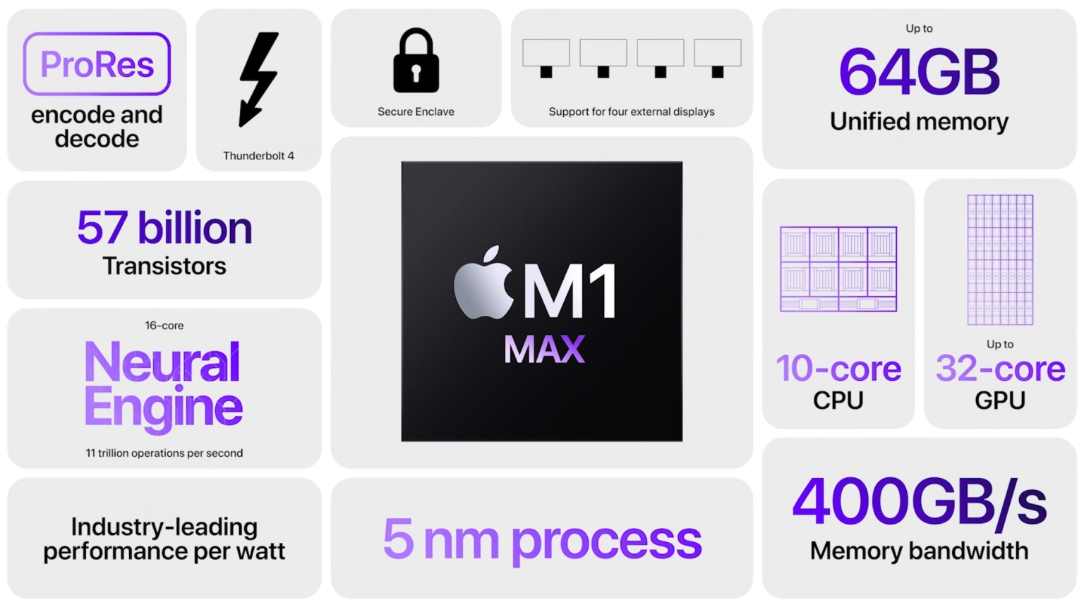
The Apple M1 Max is a System on a Chip (SoC) from Apple that is found in the late 2021 MacBook Pro 14 and 16-inch models. It offers all 10 cores available in the chip divided in eight performance cores (P-cores with 600 - 3220 MHz) and two power-efficiency cores (E-cores with 600 - 2064 MHz). There is no Turbo Boost for single cores or short burst periods. The cores are similar to the cores in the Apple M1.
The big cores (codename Firestorm) offer 192 KB instruction cache, 128 KB data cache, and 24 MB shared L2 cache (up from 12 MB in the M1). The four efficiency cores (codename Icestorm) are a lot smaller and offer only 128 KB instruction cache, 64 KB data cache, and 4 MB shared cache. CPU and GPU can both use the 48 MB SLC (System Level Cache). The efficiency cores (E cluster) clock with 600 - 2064 MHz, the performance cores (P cluster) with 600 - 3228 MHz.
The unified memory (32 or 64 GB LPDDR5-6400) next to the chip is connected by a 512 bit memory controller (200 GB/s bandwidth) and can be used by the GPU and CPU. This is the main difference to the M1 Pro and the CPU performance is quite similar.
The biggest difference to the M1 Pro is the bigger integrated GPU with 24 or 32 cores (up from 16).
Furthermore, the SoC integrates a fast 16 core neural engine, a secure enclave (e.g., for encryption), a unified memory architecture, Thunderbolt 4 controller, an ISP, and media de- and encoders (including two ProRes engines).
The M1 Pro is manufactured in 5 nm at TSMC and integrates 57 billion transistors. The peak power consumption of the chip was advertised around 30W for CPU intensive tasks.
The AMD Ryzen 3 5300U (not to be confused with the A4-5300, a CPU released in 2012) is a Lucienne family processor designed for use in thin and light laptops. The R3 5300U integrates four cores (quad core) based on the Zen 2 microarchitecture. They are clocked at 2.6 (guaranteed base clock) to 3.8 GHz (Turbo) and support SMT for a total of 8 threads. The chip is manufactured on the modern 7 nm TSMC process. Compared to the older and similar Ryzen 3 4300U (Renoir), the Ryzen 3 5300U offers SMT and slightly higher clock speeds. The faster Ryzen 3 5400U is based on the newer Zen 3 architecture. See our hub page on the Renoir Processors for more information on the Lucienne / Renoir architecture.
In addition to the four CPU cores, the APU also integrates a Radeon RX Vega 6 integrated graphics adapter with 6 CUs at up to 1500 MHz. The dual channel memory controller supports DDR4-3200 and energy efficient LPDDR4-4266 RAM. Furthermore, 4 MB level 3 cache can be found on the chip.
Performance
The average 5300U in our database matches the Core i5-11300H, the Core i7-11375H and also the Ryzen 5 4500U in multi-thread performance, making it an outstandingly good chip as far as sub-US$700 laptops go.
Your mileage may vary depending on how high the CPU power limits are and how competent the cooling solution of your system is.
Power consumption
The Ryzen 3 series chip has a default TDP of 15 W, a value that laptop makers are allowed to change to anything between 10 W and 25 W with clock speeds and performance changing accordingly as a result. By going for the lowest value possible, it will be possible to build a passively cooled system around the chip, however, most companies will do the opposite to achieve higher performance levels.
The AMD Ryzen 3 5300U is built with TSMC's 7 nm manufacturing process for average, as of mid 2023, energy efficiency.
- Range of benchmark values for this graphics card - Average benchmark values for this graphics card * Smaller numbers mean a higher performance 1 This benchmark is not used for the average calculation
v1.26
log 30. 03:26:17
#0 checking url part for id 12978 +0s ... 0s
#1 checking url part for id 13843 +0s ... 0s
#2 checking url part for id 12985 +0s ... 0s
#3 not redirecting to Ajax server +0s ... 0s
#4 did not recreate cache, as it is less than 5 days old! Created at Sun, 28 Apr 2024 05:39:51 +0200 +0.001s ... 0.001s
#5 composed specs +0.044s ... 0.045s
#6 did output specs +0s ... 0.045s
#7 getting avg benchmarks for device 12978 +0.019s ... 0.064s
#8 got single benchmarks 12978 +0.081s ... 0.145s
#9 getting avg benchmarks for device 13843 +0.003s ... 0.147s
#10 got single benchmarks 13843 +0.011s ... 0.159s
#11 getting avg benchmarks for device 12985 +0.017s ... 0.176s
#12 got single benchmarks 12985 +0.026s ... 0.202s
#13 got avg benchmarks for devices +0s ... 0.202s
#14 min, max, avg, median took s +0.445s ... 0.647s
 Deutsch
 English
 Español
 Français
 Italiano
 Nederlands
 Polski
 Português
 Русский
 Türkçe
 Svenska
 Chinese
 Magyar