

Intel Core i7-620M vs Intel Core i7-1250U vs Intel Core i5-1235U
Intel Core i7-620M
► remove from comparison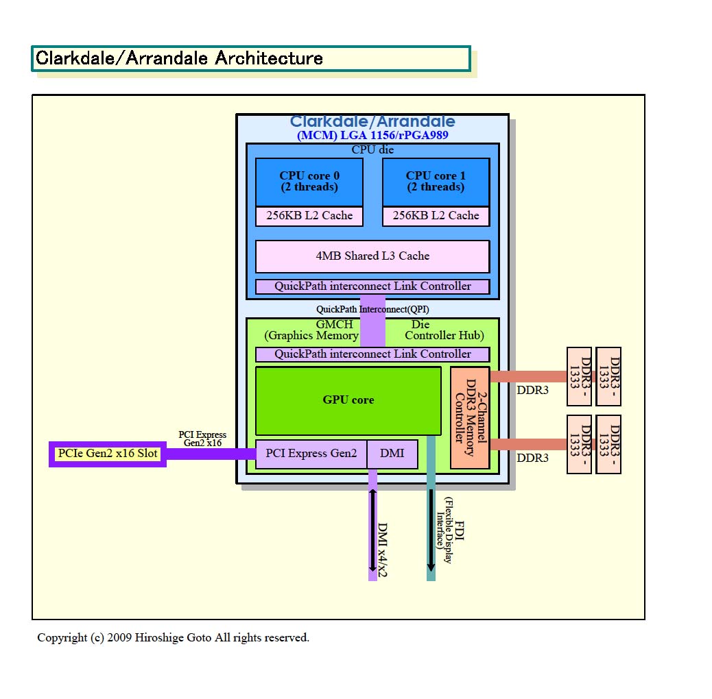
The Intel Core i7-620M is a high end dual core CPU for laptops and clocks (due to the Turbo Mode) from 2.66 to 3.33 GHz. Each core is based on the Nehalem (Westmere) micro-architecture. Hyperthreading enables the Dual Core CPU to handle 4 threads at once (for a better usage of the pipeline). Therefore, the i7-620M is related to the other i5 and i3 dual core CPUs and not the quad-core i7 CPUs.
A feature of the new Core i7-620M is the integrated graphics card called Intel HD Graphics (GMA HD) and memory controller. Both are on a separate die that is still manufactured in 45nm whereas the CPU die is already manufactured in the new 32nm process.
The performance of the Core i7-620M is on average above the former fastest mobile dual core CPU, the Core 2 Duo T9900 / X9100. In our tests, just the single threaded rendering test in the Cinebench R10 benchmark scored less points. Even the mobile Core i7-720QM quad core is slower in many cases.
The 32nm cpu cores of the Westmere generation can also process some new instructions to accelerate AES encryptions. Compared to the slower i5 versions without AES features, the 3DMark Vantage Communication Score showed a significant increase with AES enabled CPUs.
The integrated Intel Graphics Media Accelerator HD (GMA HD) graphics card is clocked with 500-733 MHz and performs clearly faster than the old GMA 4500MHD. A GeForce 9400M (ION) should still be a bit faster (especially as Nvidia and ATI cards have a better driver support than Intel up to now).
The power consumption of 35 Watt TDP (max.) counts for the whole package and therefore it is clearly better than the 35 Watt TDP of the Core 2 Duo T-series (CPU alone).
The Core i7-620M should not be mistaken with the similar named but slower low voltage and ultra low voltage chips Core i7-620LM (2.13-2.93 GHZ, 25W) and Core i7-620UM (1.2-2.26 GHz, 18 W).
Intel Core i7-1250U
► remove from comparisonThe Intel Core i7-1250U is a mobile CPU for thin and light laptops based on the Alder Lake architecture. It was announced in early 2022 and offers 2 performance cores (P-cores, Golden Cove architecture) and 8 efficient cores (E-cores, Gracemont architecture). The P-cores support Hyper-Threading leading to 12 supported threads when combined with the E-cores. The clock rate ranges from 1.1 to 4.7 GHz on the performance cluster and 0.8 to 3.5 GHz on the efficient cluster. The performance of the E-cores should be similar to old Skylake cores (compare to the Core i7-6700HQ). All cores can use up to 12 MB L3 cache. Compared to the similar Core i7-1260U, the 1250U only offers "Essentials" vPro management features.
Performance
The average 1250U in our database is in the same league as the Ryzen 5 5500U; the i5-1240U, the i7-1260U and the i7-1265U are found close nearby as well.
Thanks to its decent cooling solution and a long-term CPU power limit of 23 W, the Envy x360 13-bf0013dx is among the fastest laptops built around the 1250U that we know of. It can be at least 30% faster in CPU-bound workloads than the slowest system featuring the same chip in our database, as of August 2023.
Features
The integrated memory controller supports various memory types up to DDR5-4800, DDR4-3200, LPDDR5-5200, and LPDDR4x-4267. The Thread Director (in hardware) can support the operating system to decide which thread to use on the performance or efficient cores for the best performance. For AI tasks, the CPU also integrates GNA 3.0 and DL Boost (via AVX2). Quick Sync in version 8 is the same as in the Rocket Lake CPUs and supports MPEG-2, AVC, VC-1 decode, JPEG, VP8 decode, VP9, HEVC, and AV1 decode in hardware. The CPU only supports PCIe 4.0 (x8 for a GPU and two x4 for SSDs).
The integrated graphics adapter is based on the Xe architecture and offers all 96 EUs (Execution Units) operating at up to 0.95 GHz.
The CPU is rated at 9 W base power (TDP, PL1) and 29 W max. Turbo power (PL2) and the whole SoC is manufactured on a 10nm process at Intel, which is known as Intel 7.
Intel Core i5-1235U
► remove from comparisonThe Intel Core i5-1235U is a mid-range mobile CPU for thin and light laptops based on the Alder Lake architecture. It was announced in early 2022 and offers 2 performance cores (P-cores, Golden Cove architecture) and 8 efficient cores (E-cores, Gracemont architecture). The P-cores support Hyper-Threading leading to 12 supported threads when combined with the E-cores. The clock rate ranges from 1.3 to 4.4 GHz on the performance cluster and 0.9 to 3.3 GHz on the efficient cluster. The performance of the E-cores should be similar to old Skylake cores (compare to the Core i7-6700HQ). All cores can use up to 12 MB L3 cache. Compared to the i5-1245U, the 1235U offers lower base clock speeds and only "Essentials" vPro management features. Compared to the P-series (28W) or H-series (45W), the 15W TDP may limit the sustained performance.
Performance
The average 1235U in our database is in the same league as the Ryzen 5 PRO 5650U and also, surprisingly enough, the i7-1250U and the i7-1260U, as far as multi-thread benchmark scores are concerned. This is a very respectable result, as of mid 2023.
Thanks to its decent cooling solution and a long-term CPU power limit of 27 W, the Beelink SEi12 is among the fastest systems built around the 1235U that we know of. It can be twice as fast in CPU-bound workloads as the slowest system featuring the same chip in our database, as of August 2023.
Architecture
The integrated memory controller supports various memory types up to DDR5-4800, DDR4-3200, LPDDR5-5200, and LPDDR4x-4267. The Thread Director (in hardware) can support the operating system to decide which thread to use on the performance or efficient cores for the best performance. For AI tasks, the CPU also integrates GNA 3.0 and DL Boost (via AVX2). Quick Sync in version 8 is the same as in the Rocket Lake CPUs and supports MPEG-2, AVC, VC-1 decode, JPEG, VP8 decode, VP9, HEVC, and AV1 decode in hardware. The CPU only supports PCIe 4.0 (x8 for a GPU and two x4 for SSDs).
The integrated graphics card is based on the Xe-architecture and offers 80 of the 96 EUs (Execution Units) operating at up to 1.2 GHz.
Power consumption
This ULV processor has a Base power consumption of 15 W (also known as the long-term power limit), with 55 W being its maximum Intel-recommended Turbo power consumption. Both values are too high to allow for passively cooled designs.
Core i5-1235U is manufactured on Intel's fourth-gen 10 nm process marketed as Intel 7 for decent, as of mid-2022, energy efficiency.
| Model | Intel Core i7-620M | Intel Core i7-1250U | Intel Core i5-1235U | ||||||||||||||||||||||||||||||||||||||||||||||||||||||||||||||||||||||||||||||||||||||||||||||||||||||||||||||||||||||||||||||||||||||||||||||||||||
| Codename | Arrandale | Alder Lake-U | Alder Lake-U | ||||||||||||||||||||||||||||||||||||||||||||||||||||||||||||||||||||||||||||||||||||||||||||||||||||||||||||||||||||||||||||||||||||||||||||||||||||
| Series | Intel Core i7 | Intel Alder Lake-M | Intel Alder Lake-M | ||||||||||||||||||||||||||||||||||||||||||||||||||||||||||||||||||||||||||||||||||||||||||||||||||||||||||||||||||||||||||||||||||||||||||||||||||||
| Series: Alder Lake-M Alder Lake-U |
|
|
| ||||||||||||||||||||||||||||||||||||||||||||||||||||||||||||||||||||||||||||||||||||||||||||||||||||||||||||||||||||||||||||||||||||||||||||||||||||
| Clock | 2660 - 3333 MHz | 800 - 4700 MHz | 900 - 4400 MHz | ||||||||||||||||||||||||||||||||||||||||||||||||||||||||||||||||||||||||||||||||||||||||||||||||||||||||||||||||||||||||||||||||||||||||||||||||||||
| FSB | 2500 | ||||||||||||||||||||||||||||||||||||||||||||||||||||||||||||||||||||||||||||||||||||||||||||||||||||||||||||||||||||||||||||||||||||||||||||||||||||||
| L2 Cache | 512 KB | 9.5 MB | 9.5 MB | ||||||||||||||||||||||||||||||||||||||||||||||||||||||||||||||||||||||||||||||||||||||||||||||||||||||||||||||||||||||||||||||||||||||||||||||||||||
| L3 Cache | 4 MB | 12 MB | 12 MB | ||||||||||||||||||||||||||||||||||||||||||||||||||||||||||||||||||||||||||||||||||||||||||||||||||||||||||||||||||||||||||||||||||||||||||||||||||||
| Cores / Threads | 2 / 4 | 10 / 12 | 10 / 12 | ||||||||||||||||||||||||||||||||||||||||||||||||||||||||||||||||||||||||||||||||||||||||||||||||||||||||||||||||||||||||||||||||||||||||||||||||||||
| TDP | 35 Watt | 9 Watt | 15 Watt | ||||||||||||||||||||||||||||||||||||||||||||||||||||||||||||||||||||||||||||||||||||||||||||||||||||||||||||||||||||||||||||||||||||||||||||||||||||
| Transistors | 382+177 Million | ||||||||||||||||||||||||||||||||||||||||||||||||||||||||||||||||||||||||||||||||||||||||||||||||||||||||||||||||||||||||||||||||||||||||||||||||||||||
| Technology | 32 nm | 10 nm | 10 nm | ||||||||||||||||||||||||||||||||||||||||||||||||||||||||||||||||||||||||||||||||||||||||||||||||||||||||||||||||||||||||||||||||||||||||||||||||||||
| Die Size | 81+114 mm2 | ||||||||||||||||||||||||||||||||||||||||||||||||||||||||||||||||||||||||||||||||||||||||||||||||||||||||||||||||||||||||||||||||||||||||||||||||||||||
| max. Temp. | 105 °C | 100 °C | 100 °C | ||||||||||||||||||||||||||||||||||||||||||||||||||||||||||||||||||||||||||||||||||||||||||||||||||||||||||||||||||||||||||||||||||||||||||||||||||||
| Socket | BGA1288, PGA988 | BGA1781 | BGA1744 | ||||||||||||||||||||||||||||||||||||||||||||||||||||||||||||||||||||||||||||||||||||||||||||||||||||||||||||||||||||||||||||||||||||||||||||||||||||
| Features | Turbo Boost, Hyper Threading, Enhanced Speedstep, integrierte GMA HD 500-733MHz, Dual Channel DDR3 memory controller | LPDDR4x-4266/LPDDR5-5200 RAM, PCIe 4, Thr. Dir., DL Boost, GNA, vPro Ess., MMX, SSE, SSE2, SSE3, SSSE3, SSE4.1, SSE4.2, AVX, AVX2, BMI2, ABM, FMA, ADX, SMEP, SMAP, EIST, TM1, TM2, HT, Turbo, SST, AES-NI, RDRAND, RDSEED, SHA | DDR4-3200/LPDDR4x-4266/DDR5-4800/LPDDR5-5200 RAM, PCIe 4, Thr. Dir., DL Boost, GNA, vPro Ess., MMX SSE, SSE2, SSE3, SSSE3, SSE4.1, SSE4.2, AVX, AVX2, BMI2, ABM, FMA, ADX, SMEP, SMAP, EIST, TM1, TM2, HT, Turbo, SST, AES-NI, RDRAND, RDSEED, SHA | ||||||||||||||||||||||||||||||||||||||||||||||||||||||||||||||||||||||||||||||||||||||||||||||||||||||||||||||||||||||||||||||||||||||||||||||||||||
| Architecture | x86 | x86 | x86 | ||||||||||||||||||||||||||||||||||||||||||||||||||||||||||||||||||||||||||||||||||||||||||||||||||||||||||||||||||||||||||||||||||||||||||||||||||||
| $332 U.S. | |||||||||||||||||||||||||||||||||||||||||||||||||||||||||||||||||||||||||||||||||||||||||||||||||||||||||||||||||||||||||||||||||||||||||||||||||||||||
| Announced | |||||||||||||||||||||||||||||||||||||||||||||||||||||||||||||||||||||||||||||||||||||||||||||||||||||||||||||||||||||||||||||||||||||||||||||||||||||||
| Manufacturer | ark.intel.com | ark.intel.com | ark.intel.com | ||||||||||||||||||||||||||||||||||||||||||||||||||||||||||||||||||||||||||||||||||||||||||||||||||||||||||||||||||||||||||||||||||||||||||||||||||||
| L1 Cache | 928 KB | 928 KB | |||||||||||||||||||||||||||||||||||||||||||||||||||||||||||||||||||||||||||||||||||||||||||||||||||||||||||||||||||||||||||||||||||||||||||||||||||||
| iGPU | Intel Iris Xe Graphics G7 96EUs ( - 950 MHz) | Intel Iris Xe Graphics G7 80EUs ( - 1200 MHz) |

Benchmarks

Average Benchmarks Intel Core i7-620M → 0% n=0
Average Benchmarks Intel Core i7-1250U → 0% n=0
Average Benchmarks Intel Core i5-1235U → 0% n=0
* Smaller numbers mean a higher performance
1 This benchmark is not used for the average calculation