

Intel Core i3-N305 vs AMD Ryzen 7 5700U vs Intel Processor N100
Intel Core i3-N305
► remove from comparison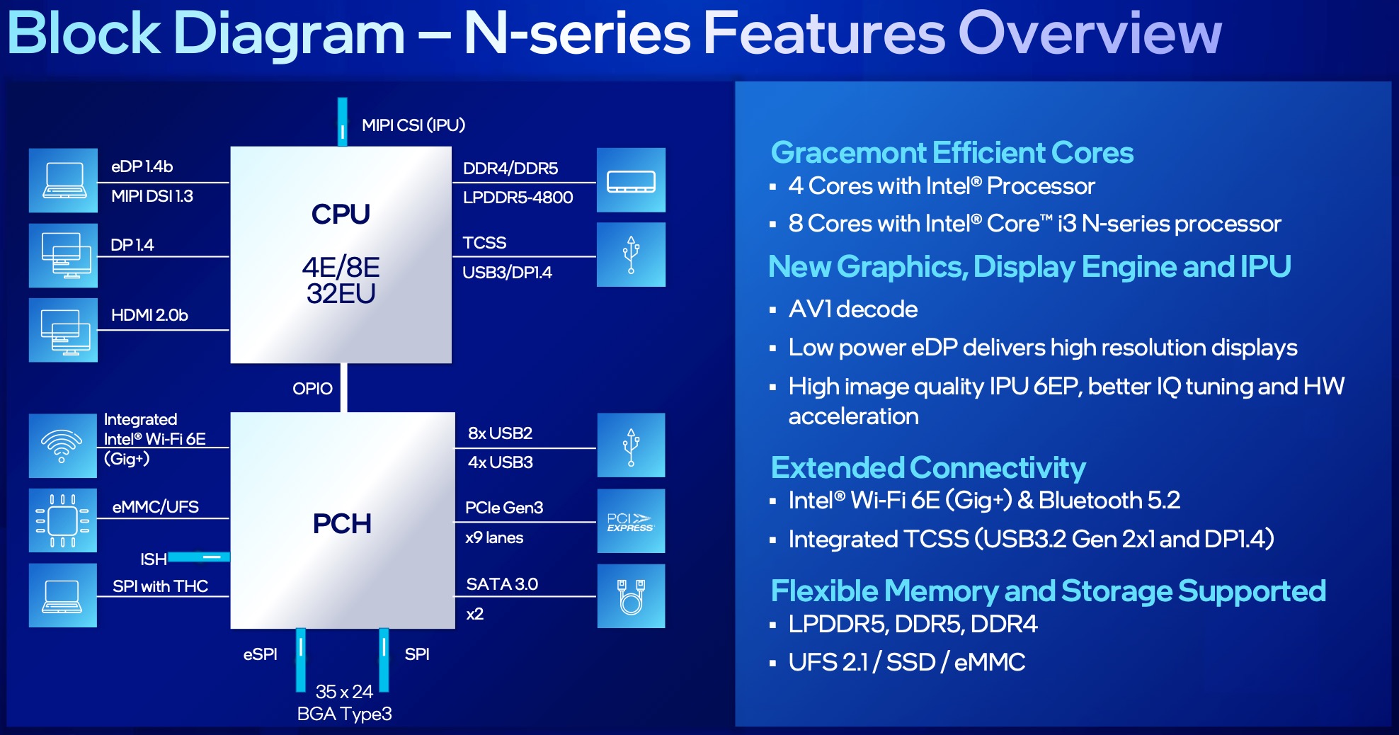
The Intel Core i3-N305 is an entry-level mobile CPU for thin and light laptops from the Alder Lake-N series. It was announced in early 2023 and offers no performance cores and 8 efficient cores (E-cores, Gracemont architecture). The chip does not support HyperThreading and clocks with up to 3.8 GHz. The performance of the E-cores should be similar to old Skylake cores (compare to the Core i7-6700HQ). All cores can use up to 6 MB L3-cache.
Performance
We have not tested a single system built around the N305, as of September 2023. Expect the chip to be 50% to 100% faster than the N95 (4 cores, 4 threads, up to 3.4 GHz).
Your mileage may vary depending on how high the CPU power limits are and how competent the cooling solutuion of your system is.
Features
The Alder Lake-N chips only support single channel memory with up to DDR5-4800, DDR4-3200 or LPDDR5-4800. The chip also supports Quick Sync and AV1 decoding (most likely same engine as in Alder Lake). Furthermore, Wi-Fi 6E and Bluetooth 5.2 are partly integrated (but no Thunderbolt). External chips can be connected via PCIe Gen3 x9 (via the PCH).
The integrated graphics adapter is based on the Xe-architecture and offersall 32 EUs (Execution Units) operating at up to 1.25 GHz. In addition to the single channel memory, the gaming performance is very limited of the iGPU.
Power consumption
The i3 has a base power consumption of 15 W and can be configured down to 9 W. The CPU is built with a further improved 10nm SuperFin process at Intel (called Intel 7).
AMD Ryzen 7 5700U
► remove from comparison
The AMD Ryzen 7 5700U is an APU of the Lucienne product family designed for leaner laptops. The Ryzen features eight Zen 2 cores clocked at 1.8 GHz (base clock speed) to 4.3 GHz (Boost) as well as a Vega 8 iGPU. Thread-doubling SMT tech is enabled in this CPU for up to 16 concurrent processing threads.
Architecture
In spite of what its name may suggest, Ryzen 7 5700U is not a Zen 3 part, meaning this is a Ryzen 4000 series mobile processor in disguise. Nevertheless, the CPU is manufactured on the modern 7 nm TSMC process and its performance as well as energy efficiency figures are very strong compared to what Intel currently has to offer in this segment.
The Ryzen 7 features 8 MB of Level 3 cache. Its built-in memory controller is designed to work with dual-channel DDR4-3200 or quad-channel LPDDR4-4266 RAM. Unlike the desktop Ryzen 5000 processors, Ryzen 7 5700U does not support PCI-Express 4.0, meaning those speedy NVMe SSDs will be limited to read/write rates of 3.9 GB/s.
The Ryzen gets soldered directly to the motherboard (FP6 socket) and is thus not user-replaceable.
Performance
The average 5700U in our database is in the same league as the Ryzen 7 4800U, Ryzen 7 PRO 5850U, Core i7-1365U, as far as multi-thread benchmark scores are concerned.
Thanks to its decent cooling solution and a long-term CPU power limit of 35 W, the Schenker VIA 15 Pro is among the fastest laptops built around the 5700U that we know of. It can be roughly 50% faster in CPU-bound workloads than the slowest system featuring the same chip in our database, as of August 2023.
Graphics
In addition to its eight CPU cores, Ryzen 7 5700U features a Radeon RX Vega series graphics adapter with 8 CUs (= 512 shaders) running at up to 1,900 MHz. This iGPU trails behind the 96 EU Intel Iris Xe Graphics G7 in synthetic benchmarks, yet its real-world performance is good enough for many games released in 2020 and 2021 at reasonable resolutions (up to Full HD 1080p) and low to medium quality. As the Vega has no VRAM of its own, it is paramount that fast system RAM is used.
The graphics adapter definitely supports UHD 2160p monitors at 60 Hz, and will gladly HW-decode AVC, HEVC and VP9-encoded videos. There is no AV1 support here though.
Power consumption
This Ryzen 7 has a default TDP, also known as the long-term power limit, of 15 W; laptop makers are free to change that to anything between 10 W and 25 W, with clock speeds and performance changing accordingly as a result. Most companies will go for a higher value to extract more performance out of the APU. By choosing the lowest value, it will be possible to build a passively cooled system around the chip, too.
The 7 nm TSMC process the R7 5700U is built with makes for decent, as of late 2022, energy efficiency.
Intel Processor N100
► remove from comparisonThe Intel Processor N100 is an entry-level mobile CPU for thin and light laptops from the Alder Lake-N series. It was announced in early 2023 and offers no performance cores and 4 of the 8 efficient cores (E-cores, Gracemont architecture). The chip does not support HyperThreading and clocks with 1 to 3.4 GHz. The performance of the E-cores should be similar to old Skylake cores (compare to the Core i7-6700HQ). All cores can use up to 6 MB L3-cache.
Performance
The average N100 in our database delivers unimpressive multi-thread benchmark scores that are most similar to those of the Core i3-1115G4. The chip is fast enough for many day-to-day tasks, but not much more than that; the other thing to keep in mind is that of the two N100-toting systems tested by us as of October 2023, both have rather high CPU power limits. The chip will be noticeably slower if limited to just six or seven Watts.
Features
The Alder Lake-N chips only support single channel memory with up to DDR5-4800, DDR4-3200 or LPDDR5-4800. The chip also supports Quick Sync and AV1 decoding (most likely same engine as in Alder Lake). Furthermore, Wi-Fi 6E and Bluetooth 5.2 are partly integrated (but no Thunderbolt). External chips can be connected via PCIe Gen3 x9 (via the PCH).
The integrated graphics adapter is based on the Xe-architecture and offers only 24 of the 32 EUs (Execution Units) operating at only 450 - 750 MHz. Due to the single channel memory, low clock speeds, and low shader count, the gaming performance of the iGPU is very limited.
Power consumption
The N100 has a base power consumption of only 6 W and is therefore suited for fanless cooling. The CPU is built with a further improved 10nm SuperFin process at Intel (called Intel 7).
| Model | Intel Core i3-N305 | AMD Ryzen 7 5700U | Intel Processor N100 | ||||||||||||||||||||||||||||||||||||||||||||||||||||||||||||||||||||
| Codename | Alder Lake-N | Lucienne-U (Zen 2) | Alder Lake-N | ||||||||||||||||||||||||||||||||||||||||||||||||||||||||||||||||||||
| Series | Intel Alder Lake-N | AMD Lucienne (Zen 2, Ryzen 5000) | Intel Alder Lake-N | ||||||||||||||||||||||||||||||||||||||||||||||||||||||||||||||||||||
| Series: Alder Lake-N Alder Lake-N |
|
|
| ||||||||||||||||||||||||||||||||||||||||||||||||||||||||||||||||||||
| Clock | 1800 - 3800 MHz | 1800 - 4300 MHz | 1000 - 3400 MHz | ||||||||||||||||||||||||||||||||||||||||||||||||||||||||||||||||||||
| L1 Cache | 768 KB | 512 KB | |||||||||||||||||||||||||||||||||||||||||||||||||||||||||||||||||||||
| L2 Cache | 4 MB | 4 MB | |||||||||||||||||||||||||||||||||||||||||||||||||||||||||||||||||||||
| L3 Cache | 6 MB | 8 MB | 6 MB | ||||||||||||||||||||||||||||||||||||||||||||||||||||||||||||||||||||
| Cores / Threads | 8 / 8 8 x 3.8 GHz Intel Gracemont E-Core | 8 / 16 | 4 / 4 4 x 3.4 GHz Intel Crestmont E-Core | ||||||||||||||||||||||||||||||||||||||||||||||||||||||||||||||||||||
| TDP | 15 Watt | 25 Watt | 6 Watt | ||||||||||||||||||||||||||||||||||||||||||||||||||||||||||||||||||||
| Technology | 10 nm | 7 nm | 10 nm | ||||||||||||||||||||||||||||||||||||||||||||||||||||||||||||||||||||
| max. Temp. | 105 °C | 105 °C | 105 °C | ||||||||||||||||||||||||||||||||||||||||||||||||||||||||||||||||||||
| Socket | BGA1264 | FP6 | BGA1264 | ||||||||||||||||||||||||||||||||||||||||||||||||||||||||||||||||||||
| Features | DDR4-3200/DDR5-4800/LPDDR5-4800 RAM (sin. chan.), PCIe 3, GNA, MMX, SSE, SSE2, SSE3, SSSE3, SSE4.1, SSE4.2, AVX, AVX2, BMI2, ABM, FMA, ADX, VMX, SMEP, SMAP, EIST, TM1, TM2, Turbo, SST, AES-NI, RDRAND, RDSEED, SHA | DDR4-3200/LPDDR4-4266 RAM, PCIe 3, MMX, SSE, SSE2, SSE3, SSSE3, SSE4A, SSE4.1, SSE4.2, AVX, AVX2, BMI2, ABM, FMA, ADX, SMEP, SMAP, SMT, CPB, AES-NI, RDRAND, RDSEED, SHA, SME | DDR4-3200/DDR5-4800/LPDDR5-4800 RAM (sin. chan.), PCIe 3, GNA, MMX, SSE, SSE2, SSE3, SSSE3, SSE4.1, SSE4.2, AVX, AVX2, BMI2, ABM, FMA, ADX, VMX, SMEP, SMAP, EIST, TM1, TM2, Turbo, SST, AES-NI, RDRAND, RDSEED, SHA | ||||||||||||||||||||||||||||||||||||||||||||||||||||||||||||||||||||
| iGPU | Intel UHD Graphics 32EUs (Alder Lake) (1000 - 1250 MHz) | AMD Radeon RX Vega 8 (Ryzen 4000/5000) ( - 1900 MHz) | Intel UHD Graphics 24EUs (Alder Lake-N) ( - 750 MHz) | ||||||||||||||||||||||||||||||||||||||||||||||||||||||||||||||||||||
| Architecture | x86 | x86 | x86 | ||||||||||||||||||||||||||||||||||||||||||||||||||||||||||||||||||||
| Announced | |||||||||||||||||||||||||||||||||||||||||||||||||||||||||||||||||||||||
| Manufacturer | ark.intel.com | www.amd.com | ark.intel.com | ||||||||||||||||||||||||||||||||||||||||||||||||||||||||||||||||||||
| $128 U.S. |

Benchmarks

Average Benchmarks Intel Core i3-N305 → 100% n=54
Average Benchmarks AMD Ryzen 7 5700U → 161% n=54
Average Benchmarks Intel Processor N100 → 75% n=54
* Smaller numbers mean a higher performance
1 This benchmark is not used for the average calculation