The Intel Core i5-7260U is a fast dual-core SoC for notebooks and Ultrabooks based on the Kaby Lake architecture and was announced in January 2017. The CPU has two processor cores clocked at 2.2-3.4 GHz (two cores also up to 3.4 GHz). The processor can execute up to four threads simultaneously thanks to Hyper Threading. It is also equipped with an Intel Iris Plus Graphics 640 GPU with 64 MB eDRAM, a dual-channel memory controller (DDR4) as well as VP9 and H.265 video decoding as well as encoding. The chip is still manufactured in a 14nm process with FinFET transistors.
Compared to the Core i7-7360U, the i5-7260 does have lower CPU (-200 MHz Turbo, -100 MHz Base) and GPU (-50 MHz) clocks.
Architecture
Intel basically uses the same micro architecture compared to Skylake, so the per-MHz performance does not differ. The manufacturer only reworked the Speed Shift technology for faster dynamic adjustments of voltages and clocks, and the improved 14nm process allows much higher frequencies combined with better efficiency than before.
Performance
At 2.2-3.4 GHz, the Core i5-7260U has much lower clocks compared to the old Core i5-6267U (2.9-3.3 GHz), but has slightly higher Turbo clocks. Similar to the 6267U, the i6-7260U can also use the 64 MB eDRAM, which should increase the performance in some scenarios.
Graphics
The integrated Intel Iris Plus 640 Graphics is the GT3e model of the Kaby Lake GPU (Intel Gen. 9.5). It has 48 Execution Units running at 300-950 MHz (i7 models up to 1050 MHz) and the performance is comparable to a GeForce 920MX thanks to fast eDRAM cache. However, there aren't any significant improvements compared to the old Iris Pro 540, so modern games can often not be played smoothly or only at the lowest or medium settings, respectively.
Contrary to Skylake, Kaby lake now also supports H.265/HEVC Main 10 with a 10-bit color depth as well as Google's VP9 codec. The dual-core Kaby Lake processors announced in January should also support HDCP 2.2.
Power Consumption
The chip is manufactured in an improved 14nm process with FinFET transistors, which improves the efficiency even further. Intel still specifies the TDP with 15 Watts, which is typical for ULV chips. Depending on the usage scenario, the TDP can vary between 7.5 (cTDP Down) and 25 Watts.
The AMD Ryzen 5 5600H is a processor for big (gaming) laptops based on the Cezanne generation. The R5 5600H has six of the eight cores based on the Zen 3 microarchitecture. They are clocked at 3.3 GHz (guaranteed base clock) to 4.2 GHz (Turbo) and support SMT for a total of 12 threads. The chip is manufactured on the modern 7 nm TSMC process.
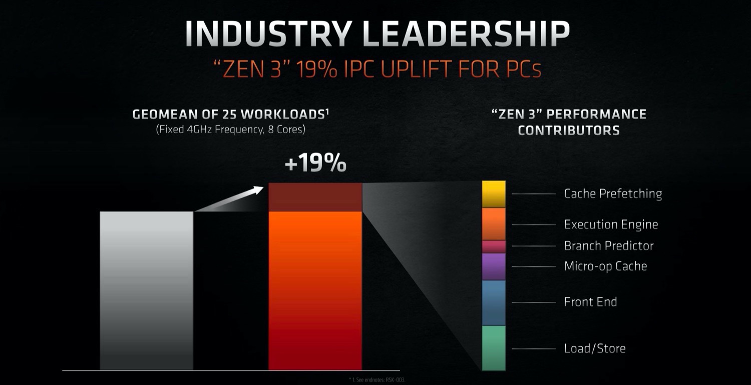
The new Zen 3 microarchitecture offers a significantly higher IPC (instructions per clock) compared to Zen 2. For desktop processors AMD claims 19 percent on average and in applications reviews showed around 12% gains at the same clock speed.
In addition to the six CPU cores, the APU also integrates a Radeon RX Vega 7 integrated graphics processor with 7 CUs running at up to 1800 MHz. The dual channel memory controller supports DDR4-3200 and energy efficient LPDDR4-4266 RAM. Furthermore, 16 MB of L3 cache can be found on the chip.
Performance
The average 5600H in our database is in the same league as the Ryzen 5 6600HS and the Core i7-1260P, as far as multi-thread benchmark scores are concerned.
Thanks to its decent cooling solution and a long-term CPU power limit of 45 W, the Lenovo Legion 5 17 is among the fastest laptops powered by the 5600H that we know of. It can be roughly 30% faster in CPU-bound workloads than the slowest system featuring the same chip in our database, as of August 2023.
Power consumption
This Ryzen 5 series chip has a default TDP (also known as the long-term power limit) of 45 W, a value that laptop makers are allowed to change to anything between 35 W and 54 W with clock speed and performance changing accordingly as a result. A high-performance cooling solution is a must for a CPU like this.
The hexa-core APU is built with the 7 nm TSMC process for decent, as of late 2022, energy efficiency.
- Range of benchmark values for this graphics card - Average benchmark values for this graphics card * Smaller numbers mean a higher performance 1 This benchmark is not used for the average calculation
v1.33
log 30. 08:35:55
#0 ran 0s before starting gpusingle class +0s ... 0s
#1 checking url part for id 8450 +0s ... 0s
#2 checking url part for id 13003 +0s ... 0s
#3 redirected to Ajax server, took 1753857354s time from redirect:1 +0s ... 0s
#4 did not recreate cache, as it is less than 5 days old! Created at Mon, 28 Jul 2025 05:17:35 +0200 +0s ... 0s
#5 composed specs +0.005s ... 0.005s
#6 did output specs +0s ... 0.005s
#7 getting avg benchmarks for device 8450 +0.001s ... 0.005s
#8 got single benchmarks 8450 +0.004s ... 0.01s
#9 getting avg benchmarks for device 13003 +0.006s ... 0.015s
#10 got single benchmarks 13003 +0.03s ... 0.045s
#11 got avg benchmarks for devices +0s ... 0.045s
#12 min, max, avg, median took s +0.048s ... 0.093s