

AMD Ryzen 5 3500U vs AMD A12-9720P
AMD Ryzen 5 3500U
► remove from comparisonThe AMD Ryzen 5 3500U is a mobile SoC that was announced in January 2019. It combines four Zen+ cores (8 threads) clocked at 2.1 GHz to 3.7 GHz with a Radeon RX Vega 8 iGPU with 8 CUs (512 Shaders) clocked at up to 1200 MHz. Specified at 15 Watt TDP, the SoC is intended for thin mid-range laptops. In Chromebooks, AMD calles the APU AMD Ryzen 5 3500C, but the specifications (and performance) are the same.
The Picasso SoC uses the Zen+ microarchitecture with slight improvements that should lead to a 3% IPS (performance per clock) improvements. Furthermore, the 12 nm process allows for higher clocks at similar power consumption.
The integrated dual-channel memory controller supports up to DDR4-2400 memory. As the features of the Picasso APUs are the same compared to the Raven Ridge predecessors, we point to our Raven Ridge launch article.
Performance
The average 3500U in our database matches the Intel Core i7-1065G7 in multi-thread performance to be an OK lower mid-range option, as of early 2021.
The Honor MagicBook 14 is among the fastest laptops powered by the 3500U that we know of. It can be up to 50% faster in CPU-bound workloads than the slowest system featuring the same chip in our database, as of August 2023.
Power consumption
This Ryzen 5 series chip has a default TDP (also known as the long-term power limit) of 15 W, a value that laptop makers are free to set to anything between 12 W and 35 W with clock speeds and performance changing accordingly as a result. Either way, this is a tad too high to allow for passively cooled designs.
The chip is manufactured on a 12 nm process for subpar, as of late 2022, energy efficiency.
AMD A12-9720P
► remove from comparison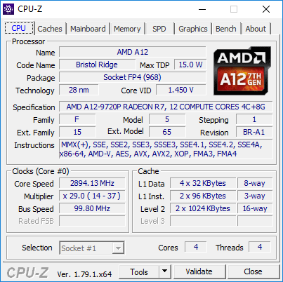
The AMD A12-9720P is a mainstream SoC from the Bristol Ridge APU series for notebooks (7th APU generation), which was introduced in 2017. The ULV chip with a TDP of 15 Watts (can be configured to 12 Watts, not verified) has four CPU cores (two Excavator modules) clocked at 2.7 - 3.8 GHz (4.05 GHz for single core were briefly achievable in our test sample), a Radeon R7 iGPU as well as a dual-channel DDR4-1866 memory controller. Carrizo is a full-fledged SoC and is also equipped with an integrated chipset, which provides all I/0 ports.
Architecture
Bristol Ridge is the successor of the Carrizo architecture and the design is almost identical. Thanks to optimized manufacturing processes and more aggressive Boost behavior, however, the clocks are a bit higher at the same power consumption. The memory controller now also supports DDR4-RAM, in this case up to 1866 MHz. More technical details are available in the following articles:
Performance
The average A12-9720P in our database is in the same league as the Core i5-4210U, as far as multi-thread benchmark scores are concerned, making the former a fairly slow chip that's suitable for basic day-to-day activities only as of late 2022.
Graphics
The integrated Radeon R7 (Bristol Ridge) GPU has 512 active shader units (8 compute cores) clocked at up to 758 MHz. Thanks to the better utilization of the clock range as well as faster DDR4-RAM, the GPU can slightly beat its predecessors Radeon R7 (Carrizo) and competes with a dedicated GeForce 920MX in the best-case scenario (dual-channel memory, low CPU requirements). Many games from 2015/2016 can be played smoothly at low settings.
Power Consumption
AMD specifies the TDP of the A12-9720P with 15 Watts, which is comparable to Intel's ULV models. This means the CPU is a good choice for thin notebooks starting with a 12-inch screen.
| Model | AMD Ryzen 5 3500U | AMD A12-9720P | ||||||||||||||||||||||||||||||||||||||||||||||||||||||||||||
| Codename | Picasso-U (Zen+) | Bristol Ridge | ||||||||||||||||||||||||||||||||||||||||||||||||||||||||||||
| Series | AMD Picasso (Ryzen 3000 APU) | AMD Bristol Ridge | ||||||||||||||||||||||||||||||||||||||||||||||||||||||||||||
| Series: Bristol Ridge Bristol Ridge |
|
| ||||||||||||||||||||||||||||||||||||||||||||||||||||||||||||
| Clock | 2100 - 3700 MHz | 2700 - 3600 MHz | ||||||||||||||||||||||||||||||||||||||||||||||||||||||||||||
| L1 Cache | 384 KB | |||||||||||||||||||||||||||||||||||||||||||||||||||||||||||||
| L2 Cache | 2 MB | 2 MB | ||||||||||||||||||||||||||||||||||||||||||||||||||||||||||||
| L3 Cache | 4 MB | |||||||||||||||||||||||||||||||||||||||||||||||||||||||||||||
| Cores / Threads | 4 / 8 | 4 / 4 | ||||||||||||||||||||||||||||||||||||||||||||||||||||||||||||
| TDP | 15 Watt | 15 Watt | ||||||||||||||||||||||||||||||||||||||||||||||||||||||||||||
| Transistors | 4500 Million | 3100 Million | ||||||||||||||||||||||||||||||||||||||||||||||||||||||||||||
| Technology | 12 nm | 28 nm | ||||||||||||||||||||||||||||||||||||||||||||||||||||||||||||
| max. Temp. | 105 °C | 90 °C | ||||||||||||||||||||||||||||||||||||||||||||||||||||||||||||
| Socket | FP5 | FP4 | ||||||||||||||||||||||||||||||||||||||||||||||||||||||||||||
| Features | DDR4-2400 RAM, PCIe 3, MMX, SSE, SSE2, SSE3, SSSE3, SSE4A, SSE4.1, SSE4.2, AVX, AVX2, BMI2, ABM, FMA, ADX, SMEP, SMAP, SMT, CPB, AES-NI, RDRAND, RDSEED, SHA, SME | DDR4-1866 RAM, PCIe 3, MMX, SSE, SSE2, SSE3, SSSE3, SSE4A, SSE4.1, SSE4.2, AVX, AVX2, BMI2, ABM, TBM, FMA4, XOP, SMEP, CPB, AES-NI, RDRAND | ||||||||||||||||||||||||||||||||||||||||||||||||||||||||||||
| iGPU | AMD Radeon RX Vega 8 (Ryzen 2000/3000) ( - 1200 MHz) | AMD Radeon R7 (Bristol Ridge) ( - 758 MHz) | ||||||||||||||||||||||||||||||||||||||||||||||||||||||||||||
| Architecture | x86 | x86 | ||||||||||||||||||||||||||||||||||||||||||||||||||||||||||||
| Announced | ||||||||||||||||||||||||||||||||||||||||||||||||||||||||||||||
| Manufacturer | www.amd.com | |||||||||||||||||||||||||||||||||||||||||||||||||||||||||||||
| Die Size | 250 mm2 |

Benchmarks

Average Benchmarks AMD Ryzen 5 3500U → 100% n=23
Average Benchmarks AMD A12-9720P → 59% n=23
* Smaller numbers mean a higher performance
1 This benchmark is not used for the average calculation