

Intel Core i7-12650H vs AMD Ryzen 5 7600 vs AMD Ryzen 9 7900
Intel Core i7-12650H
► remove from comparisonThe Intel Core i7-12650H is a high-end mobile CPU for laptops based on the Alder Lake architecture. It was announced in early 2022 and offers 6 performance cores (P-cores, Golden Cove architecture) and 4 of the 8 efficient cores (E-cores, Gracemont architecture). The P-cores support Hyper-Threading leading to 16 supported threads when combined with the E-cores. The clock rate ranges from 2.3 to 4.7 GHz on the performance cluster and 1.7 to 3.5 GHz on the efficient cluster. The performance of the E-cores should be similar to old Skylake cores (compare to the Core i7-6700HQ). All cores can use up to 24 MB L3 cache. Compared to the 12700H, the 12650H offers only 4 instead of 8 E-cores, a slower iGPU and no vPro features (for remote management).
Performance
The average 12650H in our database is in the same league as the Core i9-11950H, Ryzen 5 7640HS, Ryzen 9 5900HS, as far as multi-thread benchmark scores are concerned. This is a very good result, as of early 2023.
Thanks to its decent cooling solution and a long-term CPU power limit of 80 W, the TUF Dash F15 FX517ZR is among the fastest laptops built around the 12650H that we know of. It can be more than 25% faster in CPU-bound workloads than the slowest system featuring the same chip in our database, as of August 2023.
Features
The integrated memory controller supports various memory types up to DDR5-4800, DDR4-3200, LPDDR5-5200, and LPDDR4x-4267. The Thread Director (in hardware) can support the operating system to decide which thread to use on the performance or efficient cores for the best performance. For AI tasks, the CPU also integrates GNA 3.0 and DL Boost (via AVX2). Quick Sync in version 8 is the same as in the Rocket Lake CPUs and supports MPEG-2, AVC, VC-1 decode, JPEG, VP8 decode, VP9, HEVC, and AV1 decode in hardware. The CPU only supports PCIe 4.0 (x8 for a GPU and two x4 for SSDs).
The integrated graphics card is based on the Xe-architecture and offers 64 of the 96 EUs (Execution Units) operating at up to 1.4 GHz.
Power consumption
This Core i7 has a "minimum assured" power consumption of 35 W, with 45 W being its Base power consumption. The processor's maximum Intel-recommended Turbo power consumption sits at 115 W. It would take at least two fans to cool such a beast.
Last but not the least, Intel Core i7-12650H is built with Intel's fourth-generation 10 nm process marketed as Intel 7 for OK, as of early 2023, energy efficiency.
AMD Ryzen 5 7600
► remove from comparison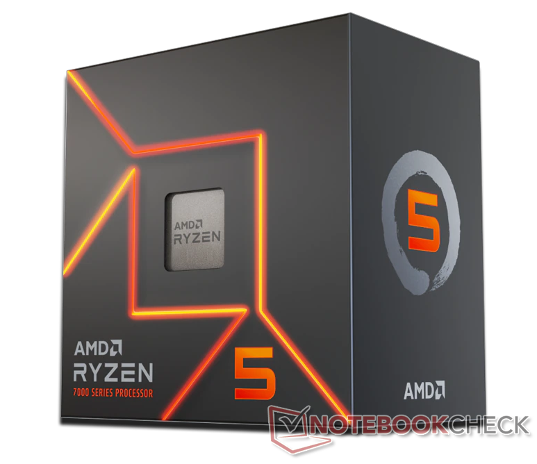
The AMD Ryzen 5 7600 is a fast mid-range desktop processor of the Raphael series. It offers 6 cores based on the Zen 4 architecture that supports hyperthreading (12 threads). The cores clock from 3.8 (base) up to 5.1 GHz (single core boost).
The Raphael series still uses a chiplet design with two CCD-clusters (each with 8 possible cores) in 5nm and an IO-die (including the memory controller and the Radeon Graphics iGPU) in 6nm.
The R5 7600X is rated at 65 Watt TDP.
AMD Ryzen 9 7900
► remove from comparison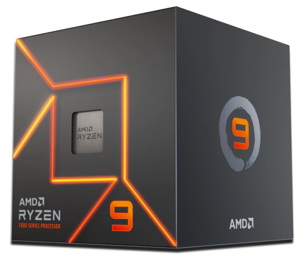
The AMD Ryzen 9 79 00 is a high-end desktop processorfrom the Raphael series with 12 cores and hyperthreading (SMT), which means it can process up to 24 threads simultaneously. Launched in early 2023, the Ryzen 9 7900 is the fastest 12-core processor with 65 watts TDP.
The Ryzen 9 7900 clocks at 3.7 GHz base clock and reaches up to 5.4 GHz on one core in Turbo mode. This is also the difference to the higher clocked Ryzen 9 7900X.
At first glance, the internal structure of the processor has not changed fundamentally. The AMD Ryzen 9 7900 is still based on the chiplet design consisting of two CCD clusters, each containing a CCX with 8 cores. However, the manufacturing process has been scaled down to 5 nm, which ensures higher clock rates. There is also the IO die, which contains the memory controller and the iGPU, among other things. This is now manufactured in a 6 nm structure width.
The AMD Ryzen 9 7900 can impress in games thanks to the significantly improved IPC.
| Model | Intel Core i7-12650H | AMD Ryzen 5 7600 | AMD Ryzen 9 7900 | ||||||||||||||||||||||||||||||||||||||||||||||||||||||||||||||||||||||||||||||||||||||||||||
| Codename | Alder Lake-H | Raphael (Zen4) | Raphael (Zen4) | ||||||||||||||||||||||||||||||||||||||||||||||||||||||||||||||||||||||||||||||||||||||||||||
| Series | Intel Alder Lake-P | AMD Raphael (Zen 4, Ryzen 7000) | AMD Raphael (Zen 4, Ryzen 7000) | ||||||||||||||||||||||||||||||||||||||||||||||||||||||||||||||||||||||||||||||||||||||||||||
| Series: Raphael (Zen 4, Ryzen 7000) Raphael (Zen4) |
|
|
| ||||||||||||||||||||||||||||||||||||||||||||||||||||||||||||||||||||||||||||||||||||||||||||
| Clock | 1700 - 4700 MHz | 3800 - 5100 MHz | 3700 - 5400 MHz | ||||||||||||||||||||||||||||||||||||||||||||||||||||||||||||||||||||||||||||||||||||||||||||
| L1 Cache | 864 KB | 384 KB | 768 KB | ||||||||||||||||||||||||||||||||||||||||||||||||||||||||||||||||||||||||||||||||||||||||||||
| L2 Cache | 9.5 MB | 6 MB | 12 MB | ||||||||||||||||||||||||||||||||||||||||||||||||||||||||||||||||||||||||||||||||||||||||||||
| L3 Cache | 24 MB | 32 MB | 64 MB | ||||||||||||||||||||||||||||||||||||||||||||||||||||||||||||||||||||||||||||||||||||||||||||
| Cores / Threads | 10 / 16 | 6 / 12 | 12 / 24 | ||||||||||||||||||||||||||||||||||||||||||||||||||||||||||||||||||||||||||||||||||||||||||||
| TDP | 45 Watt | 65 Watt | 65 Watt | ||||||||||||||||||||||||||||||||||||||||||||||||||||||||||||||||||||||||||||||||||||||||||||
| Technology | 10 nm | 5 nm | 5 nm | ||||||||||||||||||||||||||||||||||||||||||||||||||||||||||||||||||||||||||||||||||||||||||||
| max. Temp. | 100 °C | 95 °C | 95 °C | ||||||||||||||||||||||||||||||||||||||||||||||||||||||||||||||||||||||||||||||||||||||||||||
| Socket | BGA1744 | AM5 (LGA 1718) | AM5 (LGA 1718) | ||||||||||||||||||||||||||||||||||||||||||||||||||||||||||||||||||||||||||||||||||||||||||||
| Features | DDR4-3200/LPDDR4x-4266/DDR5-4800/LPDDR5-5200 RAM, PCIe 4, Thr. Dir., DL Boost, GNA, MMX, SSE, SSE2, SSE3, SSSE3, SSE4.1, SSE4.2, AVX, AVX2, BMI2, ABM, FMA, ADX, SMEP, SMAP, EIST, TM1, TM2, HT, Turbo, SST, AES-NI, RDRAND, RDSEED, SHA | MMX(+), SSE, SSE2, SSE3, SSSE3, SSE4.1, SSE4.2, SSE4A, x86-64, AMD-V, AES, AVX, AVX2, AVX512F, FMA3, SHA, Precision Boost 2 | MMX(+), SSE, SSE2, SSE3, SSSE3, SSE4.1, SSE4.2, SSE4A, x86-64, AMD-V, AES, AVX, AVX2, AVX512F, FMA3, SHA, Precision Boost 2 | ||||||||||||||||||||||||||||||||||||||||||||||||||||||||||||||||||||||||||||||||||||||||||||
| iGPU | Intel UHD Graphics 64EUs (Alder Lake 12th Gen) ( - 1400 MHz) | AMD Radeon Graphics (Ryzen 7000) (400 - 2200 MHz) | AMD Radeon Graphics (Ryzen 7000) ( - 2200 MHz) | ||||||||||||||||||||||||||||||||||||||||||||||||||||||||||||||||||||||||||||||||||||||||||||
| Architecture | x86 | x86 | x86 | ||||||||||||||||||||||||||||||||||||||||||||||||||||||||||||||||||||||||||||||||||||||||||||
| Announced | |||||||||||||||||||||||||||||||||||||||||||||||||||||||||||||||||||||||||||||||||||||||||||||||
| Manufacturer | ark.intel.com | www.amd.com | www.amd.com | ||||||||||||||||||||||||||||||||||||||||||||||||||||||||||||||||||||||||||||||||||||||||||||
| Transistors | CCD: 6,5 Mrd + IOD: 3,4 Mrd Million | 9.9 Million | |||||||||||||||||||||||||||||||||||||||||||||||||||||||||||||||||||||||||||||||||||||||||||||
| Voltage | 0.650 - 1.475V V | 0.650 - 1.475V V | |||||||||||||||||||||||||||||||||||||||||||||||||||||||||||||||||||||||||||||||||||||||||||||
| Die Size | 1x 70 (CCD) mm2 + 122 (I/O) mm2 | 262 mm2 |

Benchmarks

Average Benchmarks Intel Core i7-12650H → 100% n=38
Average Benchmarks AMD Ryzen 5 7600 → 137% n=38
Average Benchmarks AMD Ryzen 9 7900 → 187% n=38
* Smaller numbers mean a higher performance
1 This benchmark is not used for the average calculation