 Deutsch
 English
 Español
 Français
 Italiano
 Nederlands
 Polski
 Português
 Русский
 Türkçe
 Svenska
 Chinese
 Magyar
Qualcomm Adreno 685 vs Qualcomm Adreno 506 vs Qualcomm Adreno 642
Qualcomm Adreno 685
► remove from comparison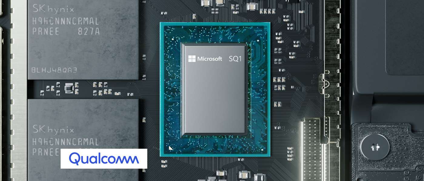
The Qualcomm Adreno 685 is an integrated graphics card in the Microsoft SQ1 ARM-based SoC. It is similar to the Adreno 680 in the Qualcomm Snapdragon 8cx SoC for Windows laptops but higher clocked and therefore with a higher theoretical performance (2 versus 1.8 TFlops).
Qualcomm Adreno 506
► remove from comparisonThe Qualcomm Adreno 506 is a mobile graphics card for mid-range smartphones and tablets (mostly Android based). It is included in the Qualcomm Snapdragon 625 SoCs and based on the Adreno 500 architecture (like the Adreno 520 in the S820, which should be fully compatible in software).
The GPU supports modern standards like Vulkan 1.0 (according to Wikipedia), OpenGL ES 3.1 + AE (3.2 in other sources), OpenCL 2.0 and DirectX 12 (FL 12.1 according to Wikipedia, 11.1 according to Qualcomm). Furthermore, the GPU supports Universal Bandwidth Compression (UBWC) to save memory bandwidth.
Qualcomm Adreno 642
► remove from comparison
The Qualcomm Adreno 642 is a smartphone and tablet GPU that is integrated within the Qualcomm Snapdragon 780G SoC. The chip will be available from mid 2021 and will be used mainly in upper mid-range Android devices.
According to Qualcomm, the Adreno 642 GPU offers a 50% improved performance over the Adreno 620, its predecessor, which is integrated in the Snapdragon 768G SoC. This is also thanks to the fast LPDDR4X-4200 memory support of the SoC.
The Adreno 642 supports OpenCL 2.0 FP, OpenGL ES 3.2 and Vulkan 1.1.
The Snapdragon 780G is manufactured in the modern 5nm LPPE process with EUV at Samsung that should provide a good power efficiency.
| Qualcomm Adreno 685 | Qualcomm Adreno 506 | Qualcomm Adreno 642 | ||||||||||||||||||||||||||||
| Adreno 600 Series |
| |||||||||||||||||||||||||||||
| Shared Memory | yes | yes | yes | |||||||||||||||||||||||||||
| API | DirectX 12 | DirectX 12.1, OpenGL ES 3.2, Vulkan | OpenGL ES 3.2 | |||||||||||||||||||||||||||
| Power Consumption | 7 Watt | |||||||||||||||||||||||||||||
| technology | 7 nm | 14 nm | 5 nm | |||||||||||||||||||||||||||
| Date of Announcement | 06.12.2018 | 15.12.2015 | 07.05.2021 | |||||||||||||||||||||||||||
| Architecture | Adreno 500 | |||||||||||||||||||||||||||||
| Core Speed | 650 MHz | |||||||||||||||||||||||||||||
| Features | OpenGL ES 3.2, OpenCL 2.0, Direct3D 12 (FL 12_1) | OpenGL ES 3.2, OpenCL 2.0, DirectX 12, Vulkan 1.1 |
|
|
| ||||||||||||||||||||||||||||||||||||||||


