 Deutsch
 English
 Español
 Français
 Italiano
 Nederlands
 Polski
 Português
 Русский
 Türkçe
 Svenska
 Chinese
 Magyar
Intel Core i7-3612QM vs AMD Ryzen 5 4680U vs AMD Ryzen 7 4980U
Intel Core i7-3612QM
► remove from comparison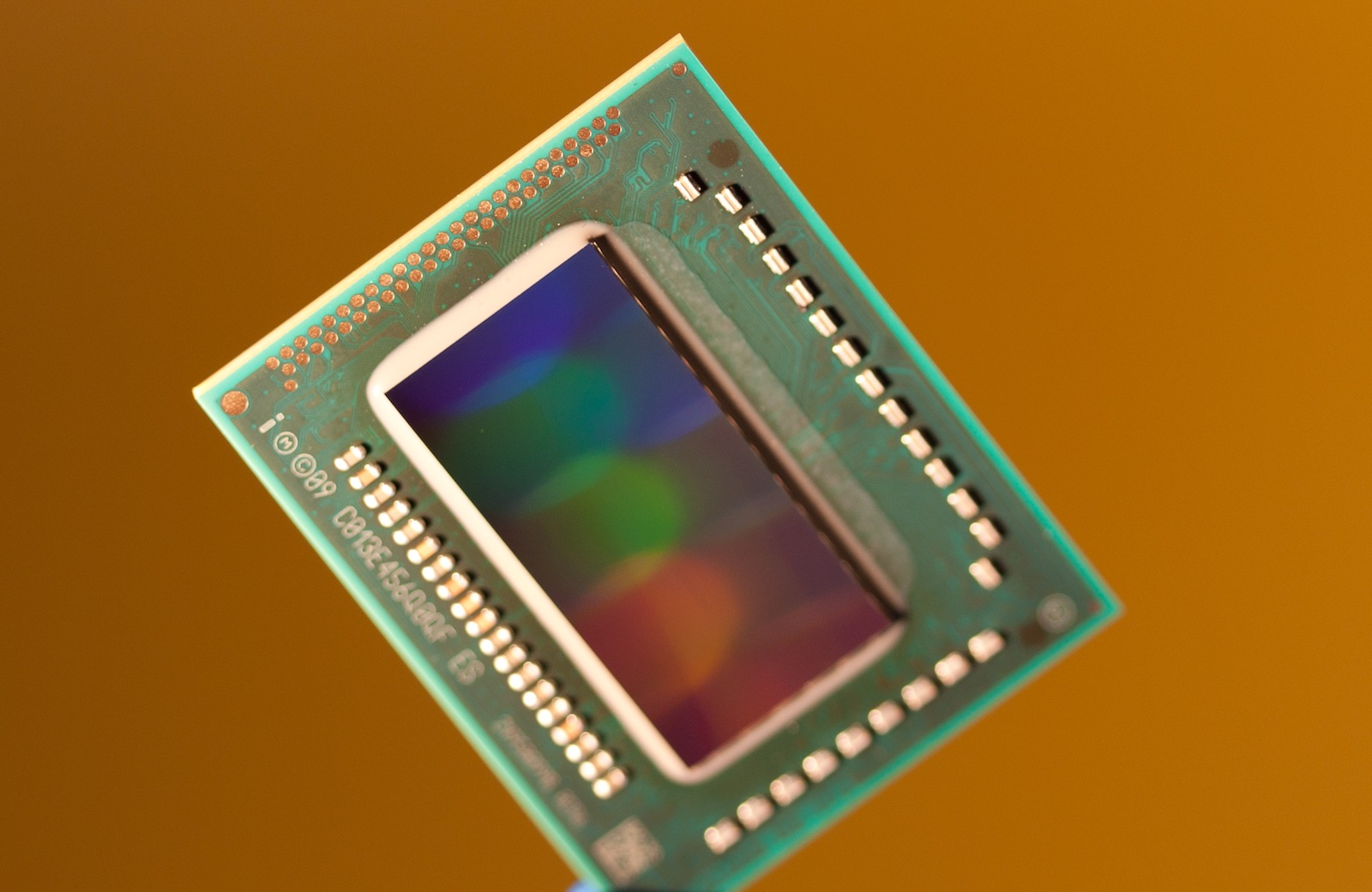
The Intel Core i7-3612QM is a fast quad-core processor for laptops based on the Ivy Bridge architecture. It is the fastest mobile processor rated at 35 Watt (at the time of announcement in mid 2012). Due to Hyperthreading, the four cores can handle up to eight threads in parallel leading to better utilization of the CPU. Each core offers a base speed of 2.1 GHz but can dynamically increase clock rates with Turbo Boost up to 2.8 GHz (for 4 active cores), 3.0 GHz (for 2 active cores) and 3.1 GHz (for 1 active core). Compared to the other quad core CPU, the 3612QM is specified at a TDP of only 35 Watt (similar to the dual-core CPUs). The BGA version (that is directly soldered to the mainboard) supports VT-d virtualization, whereas the rPGA version does not. Both dont support vPro, but otherwise all Ivy Bridge features like AES or VT-x are useable.
Ivy Bridge is an enhanced die shrink of the Sandy Bridge architecture with improvements on both GPU and CPU performance. The CPUs are produced in 22nm (versus 32nm Sandy Bridge CPUs) and are the first to introduce 3D transistors for increased energy efficiency when compared to similarly clocked Sandy Bridge processors. Other new features are integrated PCI Express 3.0 and DDR3(L)-1600 support.
The performance of the Core i7-3612QM is slightly above a similarly clocked Sandy Bridge processor due to the architectural improvements. As a result, overall performance is similar to the Sandy Bridge Core i7-2820QM. Altough the 3612QM has a higher model number than the 3610QM, it offers slower clock rates and therefore performs worse. However, the 3610QM is specified at a much higher TDP of 45 Watt.
The integrated Intel HD Graphics 4000 offers 16 Execution Units (EUs) clocked at 650 MHz up to 1100 MHz with Turbo Boost, making it one of the faster variants.
With a TDP of only 35 Watt, the Core i7-3612QM is the first quad-core CPU from Intel that is specified at the level of the dual-core mobile CPUs. Therefore, even smaller laptops can use the Core i7.
AMD Ryzen 5 4680U
► remove from comparison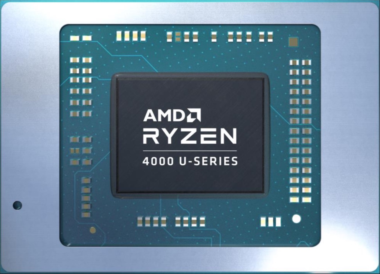
The AMD Ryzen 5 4680U is a semi-custom APU of the Renoir family designed for Microsoft devices. The 4680U integrates six CPU cores based on the Zen 2 microarchitecture clocked at 2.2 GHz (base) to 4 GHz (Boost) with SMT support for a total 12 threads. The two advantages a 4680U has over the older Ryzen 5 4600U are its higher base clock speed and a faster iGPU.
Architecture
The chip is manufactured on the modern 7 nm TSMC process and in part thanks to this fact, AMD advertises a 2x performance per watt improvement over the 12 nm Ryzen 3000 mobile processors. The built-in dual-channel memory controller supports LPDDR4-4266 RAM. Furthermore, 8 MB of L3 cache can be found on the chip.
Just like the other mobile Ryzen 4000 CPUs, a 4680U supports PCI-Express 3.0. Please go to our Renoir processor hub page for additional information on the product family.
Performance
Multi-thread performance is most comparable to the Ryzen 7 4700U and the Core i5-10500H, the latter being a much more power-hungry chip. This makes the Ryzen a more than decent CPU for most tasks, as of early 2022.
Graphics
In addition to the six CPU cores, the APU also integrates a DX 12 compatible Radeon RX Vega 7 graphics adapter with 7 CUs (448 unified shaders) at up to 1,500 MHz. The Vega iGPU will have no trouble HW-decoding AVC, HEVC and VP9 videos, but the newer AV1 codec will only be decoded via software. In terms of gaming, we are looking at an MX150-level performance. Pretty much all games released in 2020 can be played on low to medium settings in 720p on this graphics adapter.
Power consumption
This Ryzen 5 series chip has a default TDP (also known as the long-term power limit) of 15 W, a value that laptop makers - Microsoft, in this case - are free to change to anything between 10 W and 25 W, with clock speeds and performance changing accordingly as a result. Indeed, we saw the CPU consume roughly 23 watts when subjected to our usual stress testing routine.
The 7 nm TSMC process this Ryzen is built with makes for very decent, as of mid 2022, energy efficiency.
AMD Ryzen 7 4980U
► remove from comparisonThe AMD Ryzen 7 4980U is a Renoir family processor designed for certain Microsoft Surface systems. 4980U has eight Zen 2 cores clocked at 2.0 GHz (base clock speed) to 4.4 GHz (Boost) with thread-doubling SMT tech enabled for a total of 16 threads. The chip is manufactured on the modern 7 nm TSMC process and partly thanks to that AMD promises a 2x improvement in performance-per-Watt over Ryzen 3000 series mobile CPUs.
Architecture
The Zen 2 microarchitecture has brought a sizeable per-thread performance boost compared to the outgoing Zen+ parts. Renoir product family is also the first to introduce 8-core ULV processors to laptop market, keeping power consumption within reasonable limits. This AMD processor family is very impressive from most perspectives. One of the disatvantages to keep in mind is the lack of PCI-Express 4 support, meaning these blazing-fast NVMe SSDs will be limited to 3.9 GB/s tops.
Ryzen 7 4980U is designed to work with quad-channel LPDDR4 memory at up to 4,267 MHz. 8 MB of Level 3 are present in this chip. The Ryzen 7 gets soldered straight to the motherboard (FP6 socket) and is thus not user-replaceable. Please go to our Renoir hub page for more information on the product family.
Performance
The 4980U is the fastest U-class Ryzen 4000 series chip. As such, its clock speeds are 200 MHz higher (both the base one and Boost one) than what the Ryzen 7 4800U has.
It is thus hardly surprising that the average 4980U in our database is in the same league as the Ryzen 7 5800U and also the Core i7-1260P, as far as multi-thread benchmark scores are concerned.
Graphics
In addition to its eight CPU cores, the Ryzen 7 also features the Radeon RX Vega 8 graphics adapter with 8 CUs (= 512 shaders) at up to 1,950 MHz. This iGPU is compatible with FreeSync and DirectX 12 and is able to HW-decode AVC, HEVC, VP9-encoded videos (no AV1 support here). Vega 8 is capable of outputting UHD 2160p60 video signal to several monitors and, similar to Intel's Iris Xe (80 EUs), is good enough for a bit of light gaming on the go, provided one is content with sub-1080p resolutions and low/medium quailty presets.
Power consumption
The APU has a default TDP, also known as the long-term power limit, of 15 W; much like it is with other U-class Ryzen 4000 chips, AMD is fine with laptop makers (Microsoft, in this case) changing that value to anything between 10 W and 25 W.
The 7 nm TSMC process this Ryzen 7 is built with makes for above average, as of mid 2022, energy efficiency.
| Model | Intel Core i7-3612QM | AMD Ryzen 5 4680U | AMD Ryzen 7 4980U | ||||||||||||||||||||||||||||||||||||||||||||||||||||||||||||||||||||||||||||||||||||||||||||||||||||||||||||||||||||||||||||||||||||
| Series | Intel Core i7 | AMD Renoir (Ryzen 4000 APU) | AMD Renoir (Ryzen 4000 APU) | ||||||||||||||||||||||||||||||||||||||||||||||||||||||||||||||||||||||||||||||||||||||||||||||||||||||||||||||||||||||||||||||||||||
| Codename | Ivy Bridge | Renoir-U (Zen 2) | Renoir-U (Zen 2) | ||||||||||||||||||||||||||||||||||||||||||||||||||||||||||||||||||||||||||||||||||||||||||||||||||||||||||||||||||||||||||||||||||||
| Series: Renoir (Ryzen 4000 APU) Renoir-U (Zen 2) |
|
|
| ||||||||||||||||||||||||||||||||||||||||||||||||||||||||||||||||||||||||||||||||||||||||||||||||||||||||||||||||||||||||||||||||||||
| Clock | 2100 - 3100 MHz | 2200 - 4000 MHz | 2000 - 4400 MHz | ||||||||||||||||||||||||||||||||||||||||||||||||||||||||||||||||||||||||||||||||||||||||||||||||||||||||||||||||||||||||||||||||||||
| L1 Cache | 256 KB | 384 KB | 512 KB | ||||||||||||||||||||||||||||||||||||||||||||||||||||||||||||||||||||||||||||||||||||||||||||||||||||||||||||||||||||||||||||||||||||
| L2 Cache | 1 MB | 3 MB | 4 MB | ||||||||||||||||||||||||||||||||||||||||||||||||||||||||||||||||||||||||||||||||||||||||||||||||||||||||||||||||||||||||||||||||||||
| L3 Cache | 6 MB | 8 MB | 8 MB | ||||||||||||||||||||||||||||||||||||||||||||||||||||||||||||||||||||||||||||||||||||||||||||||||||||||||||||||||||||||||||||||||||||
| Cores / Threads | 4 / 8 | 6 / 12 | 8 / 16 | ||||||||||||||||||||||||||||||||||||||||||||||||||||||||||||||||||||||||||||||||||||||||||||||||||||||||||||||||||||||||||||||||||||
| TDP | 35 Watt | 15 Watt | 15 Watt | ||||||||||||||||||||||||||||||||||||||||||||||||||||||||||||||||||||||||||||||||||||||||||||||||||||||||||||||||||||||||||||||||||||
| Transistors | 1400 Million | ||||||||||||||||||||||||||||||||||||||||||||||||||||||||||||||||||||||||||||||||||||||||||||||||||||||||||||||||||||||||||||||||||||||
| Technology | 22 nm | 7 nm | 7 nm | ||||||||||||||||||||||||||||||||||||||||||||||||||||||||||||||||||||||||||||||||||||||||||||||||||||||||||||||||||||||||||||||||||||
| Die Size | 160 mm2 | ||||||||||||||||||||||||||||||||||||||||||||||||||||||||||||||||||||||||||||||||||||||||||||||||||||||||||||||||||||||||||||||||||||||
| max. Temp. | 105 °C | 105 °C | 105 °C | ||||||||||||||||||||||||||||||||||||||||||||||||||||||||||||||||||||||||||||||||||||||||||||||||||||||||||||||||||||||||||||||||||||
| Socket | FCBGA1224, FCPGA988 | FP6 | FP6 | ||||||||||||||||||||||||||||||||||||||||||||||||||||||||||||||||||||||||||||||||||||||||||||||||||||||||||||||||||||||||||||||||||||
| Features | HD Graphics 4000 (650-1100MHz), DDR3(L)-1600 Memory Controller, HyperThreading, AVX, Quick Sync, Virtualization | LPDDR4-4266 RAM, PCIe 3, MMX, SSE, SSE2, SSE3, SSSE3, SSE4A, SSE4.1, SSE4.2, AVX, AVX2, BMI2, ABM, FMA, ADX, SMEP, SMAP, SMT, CPB, AES-NI, RDRAND, RDSEED, SHA | LPDDR4-4266 RAM, PCIe 3, MMX, SSE, SSE2, SSE3, SSSE3, SSE4A, SSE4.1, SSE4.2, AVX, AVX2, BMI2, ABM, FMA, ADX, SMEP, SMAP, SMT, CPB, AES-NI, RDRAND, RDSEED, SHA | ||||||||||||||||||||||||||||||||||||||||||||||||||||||||||||||||||||||||||||||||||||||||||||||||||||||||||||||||||||||||||||||||||||
| iGPU | Intel HD Graphics 4000 (650 - 1100 MHz) | AMD Radeon RX Vega 7 ( - 1500 MHz) | AMD Radeon RX Vega 8 (Ryzen 4000/5000) ( - 1950 MHz) | ||||||||||||||||||||||||||||||||||||||||||||||||||||||||||||||||||||||||||||||||||||||||||||||||||||||||||||||||||||||||||||||||||||
| Architecture | x86 | x86 | x86 | ||||||||||||||||||||||||||||||||||||||||||||||||||||||||||||||||||||||||||||||||||||||||||||||||||||||||||||||||||||||||||||||||||||
| Announced | |||||||||||||||||||||||||||||||||||||||||||||||||||||||||||||||||||||||||||||||||||||||||||||||||||||||||||||||||||||||||||||||||||||||
| Manufacturer | ark.intel.com | www.amd.com | www.amd.com |
