The Intel Core i5-12450H is a high-end mobile CPU for laptops based on the Alder Lake architecture. It was announced in early 2022 and offers 4 of the 6 performance cores (P-cores, Golden Cove architecture) and 4 of the 8 efficient cores (E-cores, Gracemont architecture) leading to 8 cores in total (octa core CPU). The P-cores support Hyper-Threading leading to 12 supported threads when combined with the E-cores. The clock rate ranges from 2 to 4.4 GHz on the performance cluster and 1.5 to 3.3 GHz on the efficient cluster. The performance of the E-cores should be similar to old Skylake cores (compare to the Core i7-6700HQ). All cores can use up to 12 MB L3 cache. Compared to the 12500H, the 12450H offers less E-cores, lower clock rates, a slower iGPU and no vPro support.
Performance
The average 12450H in our extensive database is a bit of a disappointment, its multi-thread benchmark scores only just matching those of the Ryzen 7 5700U and the Core i7-10750H, both fairly old chips as of Q2 2023.
Your mileage may vary depending on how high the CPU power limits are and how competent the cooling solution of your system is.
Features
The integrated memory controller supports various memory types up to DDR5-4800, DDR4-3200, LPDDR5-5200, and LPDDR4x-4267. The Thread Director (in hardware) can support the operating system to decide which thread to use on the performance or efficient cores for the best performance. For AI tasks, the CPU also integrates GNA 3.0 and DL Boost (via AVX2). Quick Sync in version 8 is the same as in the Rocket Lake CPUs and supports MPEG-2, AVC, VC-1 decode, JPEG, VP8 decode, VP9, HEVC, and AV1 decode in hardware. The CPU only supports PCIe 4.0 (x8 for a GPU and two x4 for SSDs).
The integrated graphics adapter is based on the Xe-architecture and offers 48 of the 96 EUs (Execution Units) operating at up to 1.2 GHz.
The CPU is rated at 45 W base power (95 W PL2) but most laptops will use a PL1 of around 60 Watt. The SoC is manufactured in a 10nm process at Intel, which is known as Intel 7.
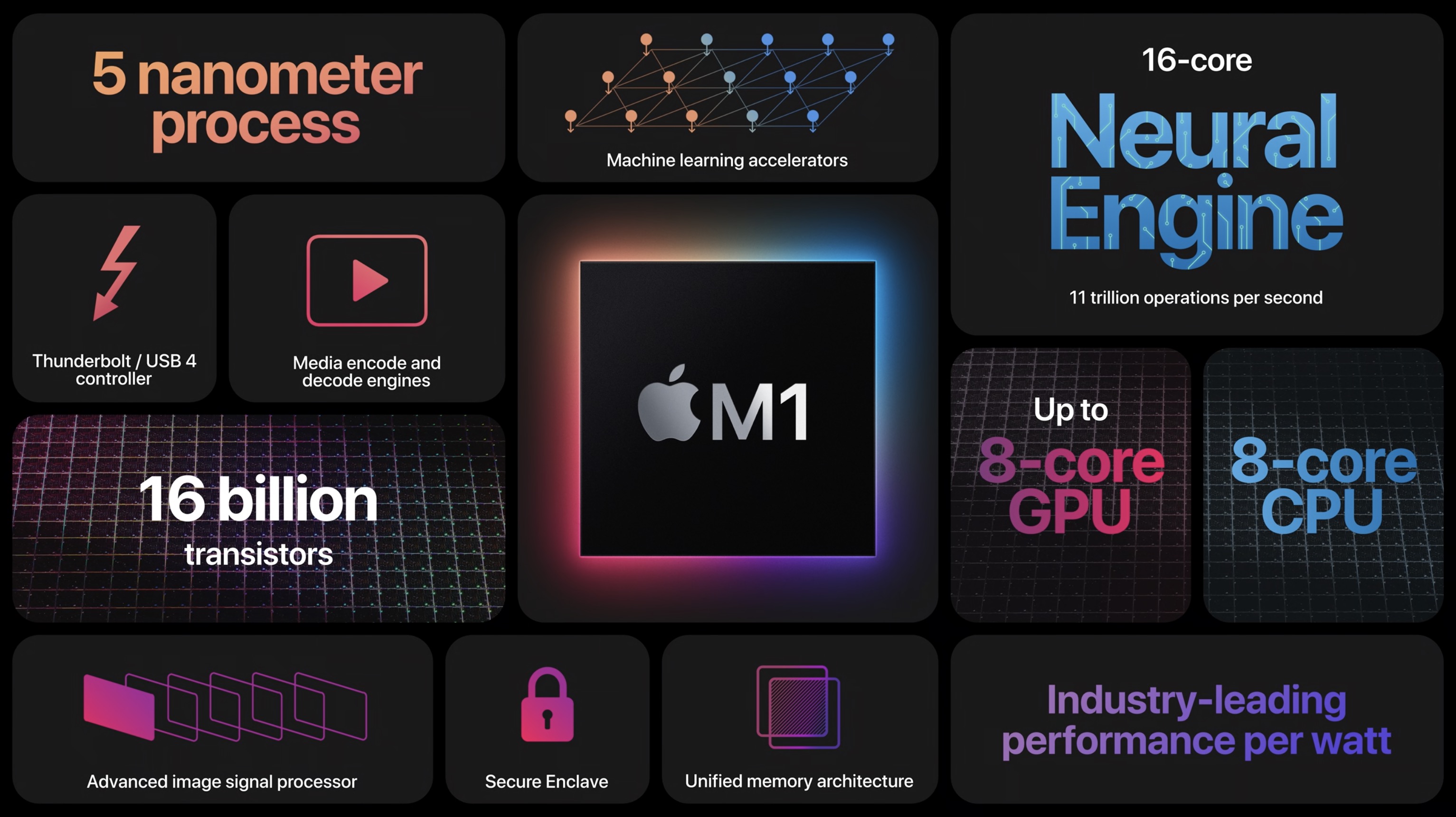
The Apple M1 is a System on a Chip (SoC) from Apple that is found in the late 2020 MacBook Air, MacBook Pro 13, and Mac Mini. It offers 8 cores divided in four performance cores and four power-efficiency cores. The big cores offer 192 KB instruction cache, 128 KB data cache, and 12 MB shared L2 cache. According to Apple the performance of these cores should be better than anything on the market (in late 2020). The four efficiency cores are a lot smaller and offer only 128 KB instruction cache, 64 KB data cache, and 4 MB shared cache. The efficiency cores (E cluster) clock with 600 - 2064 MHz, the performance cores (P cluster) with 600 - 3204 MHz.
The M1 is available in two TDP variants, a passive cooled 10 Watt variant for the MacBook Air and an active cooled faster variant for the MacBook Pro 13 and Mac Mini. Those should offer a better-sustained performance according to Apple.
The integrated graphics card in the M1 offers 8 cores (7 cores in the entry MacBook Air) and a peak performance of 2.6 teraflops. Apple claims that it is faster than any other iGPU at the time of announcement.
Furthermore, the SoC integrates a fast 16 core neural engine with a peak performance of 11 TOPS (for AI hardware acceleration), a secure enclave (e.g., for encryption), a unified memory architecture, Thunderbolt / USB 4 controller, an ISP, and media de- and encoders.
The Apple M1 includes 16 billion transistors (up from the 10 billion of the A12Z Bionic and therefore double the amount of a Tiger Lake-U chip like the i7-1185G7) and is manufactured in 5nm at TSMC.
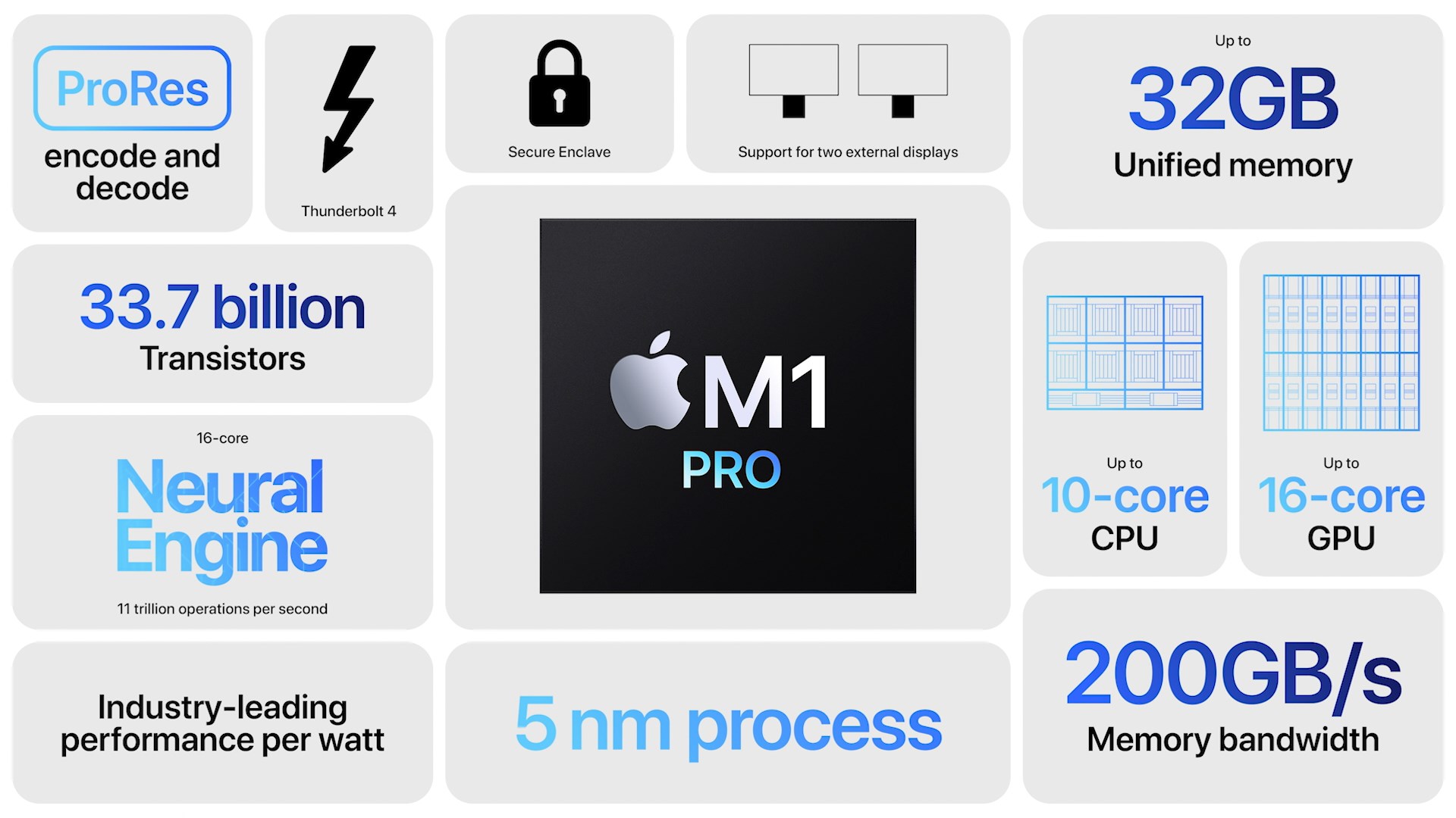
The Apple M1 Pro 8-Core is a System on a Chip (SoC) from Apple that is found in the late 2021 MacBook Pro 14 and 16-inch models. It offers 8 cores from the 10 available in the chip divided in six performance cores (P-cores with 600 - 3220 MHz) and four power-efficiency cores (E-cores with 600 - 2064 MHz). The cores are similar to the cores in the Apple M1.
The big cores (codename Firestorm) offer 192 KB instruction cache, 128 KB data cache, and 24 MB shared L2 cache (up from 12 MB in the M1). The four efficiency cores (codename Icestorm) are a lot smaller and offer only 128 KB instruction cache, 64 KB data cache, and 4 MB shared cache. Finally, the SoC includes 16 MB System Level Cache shared by the GPU. The efficiency cores (E cluster) clock with 600 - 2064 MHz, the performance cores (P cluster) with 600 - 3228 MHz.
The unified memory (16 or 32 GB LPDDR5-6400) next to the chip is connected by a 256 bit memory controller and can be used by the GPU and CPU.
Furthermore, the SoC integrates a fast 16 core neural engine, a secure enclave (e.g., for encryption), a unified memory architecture, Thunderbolt 4 controller, an ISP, and media de- and encoders (including ProRes).
The M1 Pro is manufactured in 5 nm at TSMC and integrates 33.7 billion transistors. The peak power consumption of the chip was advertised around 30W for CPU intensive tasks.
- Range of benchmark values for this graphics card - Average benchmark values for this graphics card * Smaller numbers mean a higher performance 1 This benchmark is not used for the average calculation
v1.33
log 15. 04:21:11
#0 ran 0s before starting gpusingle class +0s ... 0s
#1 checking url part for id 14057 +0s ... 0s
#2 checking url part for id 12937 +0s ... 0s
#3 checking url part for id 13847 +0s ... 0s
#4 redirected to Ajax server, took 1755224471s time from redirect:0 +0s ... 0s
#5 did not recreate cache, as it is less than 5 days old! Created at Wed, 13 Aug 2025 05:18:40 +0200 +0s ... 0s
#6 composed specs +0.006s ... 0.006s
#7 did output specs +0s ... 0.006s
#8 getting avg benchmarks for device 14057 +0.001s ... 0.008s
#9 got single benchmarks 14057 +0.002s ... 0.01s
#10 getting avg benchmarks for device 12937 +0.001s ... 0.011s
#11 got single benchmarks 12937 +0.008s ... 0.019s
#12 getting avg benchmarks for device 13847 +0.001s ... 0.019s
#13 got single benchmarks 13847 +0.004s ... 0.023s
#14 got avg benchmarks for devices +0s ... 0.023s
#15 min, max, avg, median took s +0.037s ... 0.06s