

AMD Ryzen 7 6800U vs Intel Core i9-12900HK vs Intel Core i5-12600H
AMD Ryzen 7 6800U
► remove from comparison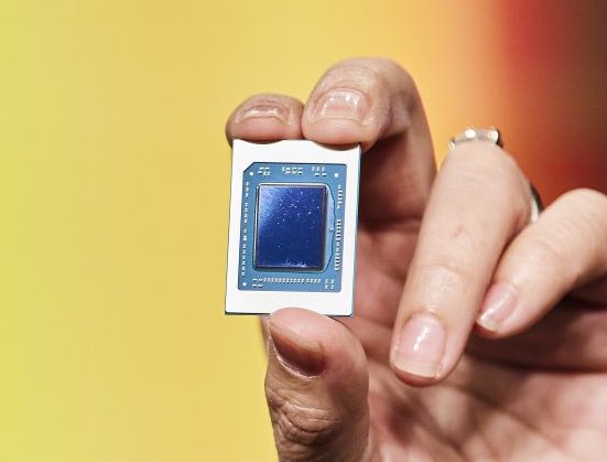
The AMD Ryzen 7 6800U is a processor for thin and light laptops based of the Rembrandt generation. The R7 6800U integrates all eight cores based on the Zen 3+ microarchitecture. They are clocked at 2.7 (guaranteed base clock) to 4.7 GHz (Turbo) and support SMT / Hyperthreading (16 threads). The chip is manufactured on the modern 6 nm TSMC process. Compared to the similar R7 6800H, the 6800U offers a lower base clock speed and a lower TDP.
The new Zen 3+ is a refresh of the Zen 3 architecture and should not offer a lot of changes. The chip itself however, offers a lot of new features, like support for USB 4 (40 Gbps), PCI-E Gen 4, DDR5-4800MT/s or LPDDR5-6400MT/s, WiFi 6E, Bluetooth LE 5.2, DisplayPort 2, and AV1 decode.
A big novelty is the integrated GPU Radeon 680M, that is now based on the RDNA2 architecture and offers 12 CUs at up to 2.2 GHz. It should be the fastest iGPU of all at the time of announcement.
Performance
The average 6800U in our database easily shoulders its way towards the best of the best, trading blows with the Core i7-1270P, the Core i7-11850H and the Ryzen 7 PRO 6850H as far as multi-thread benchmark scores are concerned. Throw everything you can at this little guy. He'll take it all and ask for more.
Thanks to its decent cooling solution and a long-term CPU power limit of more than 20 W, the Mercury EM680 is among the fastest systems built around the 6800U that we know of. It can be at least 20% faster in CPU-bound workloads than the slowest system featuring the same chip in our database, as of August 2023.
Power consumption
This Ryzen 7 series chip has a default TDP, also known as the long-term power limit, of 15 W to 28 W, the expectation being that laptop makers will go for a higher value in exchange for higher performance. Either way, a proper cooling solution is a must.
The R7 6800U is manufactured on the 6 nm TSMC process for higher-than-average, as of mid 2023, energy efficiency.
Intel Core i9-12900HK
► remove from comparisonThe Intel Core i9-12900HK is a high-end mobile CPU for laptops based on the Alder Lake architecture. It was announced in early 2022 and offers 6 performance cores (P-cores, Golden Cove architecture) and 8 efficient cores (E-cores, Gracemont architecture). The P-cores support Hyper-Threading leading to 20 supported threads when combined with the E-cores. The clock rate ranges from 2.5 to 5 GHz on the performance cluster and 1.8 to 3.8 GHz on the efficiency cluster. The performance of the E-cores should be similar to old Skylake cores (compare with the Core i7-6920HQ). All cores can use up to 24 MB L3 cache. As a K-variant, the CPU offers an open multiplicator and therefore the possibility to overclock the CPU cores. Compared to the similar i9-12900H, the 12900HK only offers the "Essentials" features of vPro.
Performance
The average 12900HK in our database is in the same as the Core i9-13900H, as far as multi-thread benchmark scores are concerned. It's also almost as fast as the Ryzen 7 7745HX and the Core i5-13500HX. This is a super-fast processor, as of mid 2023; it will have no issues running any app or any game for at least two more years.
Thanks to its decent cooling solution and a long-term CPU power limit of 134 W, the Alienware x17 R2 P48E is among the fastest laptops built around the 12900HK that we know of. It can be more than 40% faster in CPU-bound workloads than the slowest system featuring the same chip in our database, as of August 2023.
Features
The integrated memory controller supports various memory types up to DDR5-4800, DDR4-3200, LPDDR5-5200, and LPDDR4x-4267. The Thread Director (in hardware) can support the operating system to decide which thread to use on the performance or efficient cores for the best performance. For AI tasks, the CPU also integrates GNA 3.0 and DL Boost (via AVX2). Quick Sync in version 8 is the same as in the Rocket Lake CPUs and supports MPEG-2, AVC, VC-1 decode, JPEG, VP8 decode, VP9, HEVC, and AV1 decode in hardware. The CPU only supports PCIe 4.0 (x8 for a GPU and two x4 for SSDs).
The integrated graphics card is based on the Xe-architecture and offers 96 EUs (Execution Units) operating at up to 1.45 GHz.
Power consumption
This Core i9 series chip has a "minimum assured" power consumption of 35 W, with 45 W being its Base power consumption. The maximum Intel-recommended Turbo power consumption sits at 115 W.
The i9-12900HK is manufactured on Intel's 4th generation 10 nm process marketed as Intel 7 for lower-than-average, as of mid-2023, energy efficiency.
Intel Core i5-12600H
► remove from comparisonThe Intel Core i5-12600H is a high-end mobile CPU for laptops based on the Alder Lake architecture. It was announced in early 2022 and offers 4 of the 6 performance cores (P-cores, Golden Cove architecture) and all 8 efficient cores (E-cores, Gracemont architecture). The P-cores support Hyper-Threading leading to 16 supported threads when combined with the E-cores. The clock rate ranges from 2.7 to 4.5 GHz on the performance cluster and 2 to 3.3 GHz on the efficient cluster. The performance of the E-cores should be similar to old Skylake cores (compare to the Core i7-6700HQ). All cores can use up to 18 MB L3 cache. Compared to the 12650H, the 12600H offers less P-cores but more E-cores, a faster iGPU and "Enterprise" vPro features (for remote management).
Performance
Thanks to the 12 cores, the multi-threaded performance should be clearly faster than the older Tiger Lake-H CPUs with similar clock speeds (especially like the Core i5-11500H with only 6 cores). Due to the architectural improvements, single-core performance is also better than similar or higher clocked Tiger Lake CPUs.
Features
The integrated memory controller supports various memory types up to DDR5-4800, DDR4-3200, LPDDR5-5200, and LPDDR4x-4267. The Thread Director (in hardware) can support the operating system to decide which thread to use on the performance or efficient cores for the best performance. For AI tasks, the CPU also integrates GNA 3.0 and DL Boost (via AVX2). Quick Sync in version 8 is the same as in the Rocket Lake CPUs and supports MPEG-2, AVC, VC-1 decode, JPEG, VP8 decode, VP9, HEVC, and AV1 decode in hardware. The CPU only supports PCIe 4.0 (x8 for a GPU and two x4 for SSDs).
The integrated graphics card is based on the Xe-architecture and offers 80 of the 96 EUs (Execution Units) operating at up to 1.4 GHz.
The CPU is rated at 45 W base power (95 W PL2) but most laptops will use a PL1 of around 60 Watt. The SoC is manufactured in a 10nm process at Intel, which is known as Intel 7.
| Model | AMD Ryzen 7 6800U | Intel Core i9-12900HK | Intel Core i5-12600H | ||||||||||||||||||||||||||||||||||||||||||||||||||||||||||||||||
| Codename | Rembrandt-U (Zen 3+) | Alder Lake-H | Alder Lake-H | ||||||||||||||||||||||||||||||||||||||||||||||||||||||||||||||||
| Series | AMD Rembrandt (Zen 3+) | Intel Alder Lake-P | Intel Alder Lake-P | ||||||||||||||||||||||||||||||||||||||||||||||||||||||||||||||||
| Series: Alder Lake-P Alder Lake-H |
|
|
| ||||||||||||||||||||||||||||||||||||||||||||||||||||||||||||||||
| Clock | 2700 - 4700 MHz | 1800 - 5000 MHz | 2000 - 4500 MHz | ||||||||||||||||||||||||||||||||||||||||||||||||||||||||||||||||
| L1 Cache | 512 KB | 1.2 MB | 1.1 MB | ||||||||||||||||||||||||||||||||||||||||||||||||||||||||||||||||
| L2 Cache | 4 MB | 11.5 MB | 10 MB | ||||||||||||||||||||||||||||||||||||||||||||||||||||||||||||||||
| L3 Cache | 16 MB | 24 MB | 18 MB | ||||||||||||||||||||||||||||||||||||||||||||||||||||||||||||||||
| Cores / Threads | 8 / 16 | 14 / 20 | 12 / 16 | ||||||||||||||||||||||||||||||||||||||||||||||||||||||||||||||||
| TDP | 28 Watt | 45 Watt | 45 Watt | ||||||||||||||||||||||||||||||||||||||||||||||||||||||||||||||||
| Technology | 6 nm | 10 nm | 10 nm | ||||||||||||||||||||||||||||||||||||||||||||||||||||||||||||||||
| max. Temp. | 95 °C | 100 °C | 100 °C | ||||||||||||||||||||||||||||||||||||||||||||||||||||||||||||||||
| Socket | FP7/FP7r2 | BGA1744 | BGA1744 | ||||||||||||||||||||||||||||||||||||||||||||||||||||||||||||||||
| Features | DDR5-4800/LPDDR5-6400 RAM (incl. ECC), PCIe 4, MMX, SSE, SSE2, SSE3, SSSE3, SSE4A, SSE4.1, SSE4.2, AVX, AVX2, BMI2, ABM, FMA, ADX, SMEP, SMAP, SMT, CPB, AES-NI, RDRAND, RDSEED, SHA, SME | DDR4-3200/LPDDR4x-4266/DDR5-4800/LPDDR5-5200 RAM, PCIe 4, Thr. Director, DL Boost, GNA, vPro Ess., MMX, SSE, SSE2, SSE3, SSSE3, SSE4.1, SSE4.2, AES, AVX, AVX2, FMA3, SHA | DDR4-3200/LPDDR4x-4266/DDR5-4800/LPDDR5-5200 RAM, PCIe 4, Thr. Dir., DL B,., GNA, vPro En., RPE, MMX, SSE, SSE2, SSE3, SSSE3, SSE4.1, SSE4.2, AVX, AVX2, BMI2, ABM, FMA, ADX, VMX, SMX, SMEP, SMAP, EIST, TM1, TM2, HT, Turbo, SST, AES-NI, RDRAND, RDSEED, SHA | ||||||||||||||||||||||||||||||||||||||||||||||||||||||||||||||||
| iGPU | AMD Radeon 680M ( - 2200 MHz) | Intel Iris Xe Graphics G7 96EUs ( - 1450 MHz) | Intel Iris Xe Graphics G7 80EUs ( - 1400 MHz) | ||||||||||||||||||||||||||||||||||||||||||||||||||||||||||||||||
| Architecture | x86 | x86 | x86 | ||||||||||||||||||||||||||||||||||||||||||||||||||||||||||||||||
| Announced | |||||||||||||||||||||||||||||||||||||||||||||||||||||||||||||||||||
| Manufacturer | www.amd.com | ark.intel.com | ark.intel.com |

Benchmarks

Average Benchmarks AMD Ryzen 7 6800U → 0% n=0
Average Benchmarks Intel Core i9-12900HK → 0% n=0
* Smaller numbers mean a higher performance
1 This benchmark is not used for the average calculation