 Deutsch
 English
 Español
 Français
 Italiano
 Nederlands
 Polski
 Português
 Русский
 Türkçe
 Svenska
 Chinese
 Magyar
Intel Pentium Silver N5000 vs AMD A9-9425 vs AMD A6-9220e
Intel Pentium Silver N5000
► remove from comparison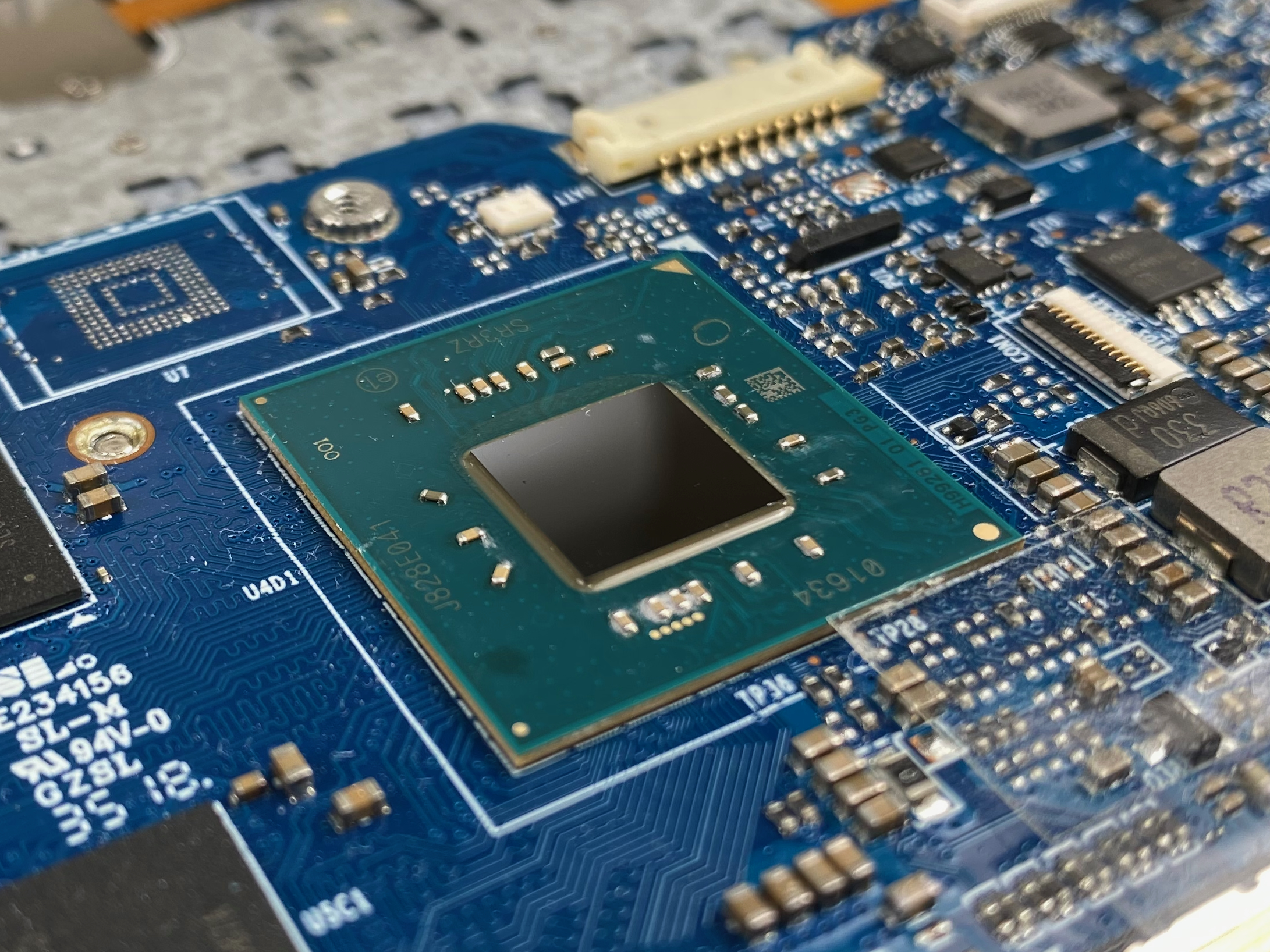
The Intel Pentium Silver N5000 is a quad-core SoC primarily for inexpensive notebooks and was announced late 2017. It runs at 1.1-2.7 GHz (Single Core Burst, Multi Core Burst max. 2.6 GHz) and is based on the Gemini Lake platform. Similar to the Apollo Lake predecessor, the chip is manufactured in a 14 nm process with FinFETs but offers slightly improved processor cores, double the amount of L2 cache, a smaller package, a new generation of monitor outputs (Gen 10) and a partly integrated WiFi chip. Besides four CPU cores, the chip also includes a DirectX 12 capable GPU as well as a DDR4/LPDDR4 memory controller (dual-channel, up to 2400 MHz). The SoC is not replaceable as it is directly soldered to the mainboard.
Architecture
The processor architecture was slightly reworked and is now called Goldmont Plus. It features an increased level 2 cache (to 4 MB). That means the per-clock-performance should be a bit better, but not near the Core CPUs like Kaby Lake Y.
Performance
The average N5000 in our database is in the same league as the AMD 3050e and the Pentium 4415U, as far as multi-thread benchmark scores are concerned. This is a really poor result, as of Q3 2023.
The Yoga 330-11IGM is among the fastest laptops featuring the N5000 that we know of. It can be more than 30% faster in CPU-bound workloads than the slowest system built around the same chip in our database, as of August 2023.
GPU Performance
The UHD Graphics 605 (Gemini Lake) is based on Intel's Gen9 architecture, which supports DirectX 12 and is also used for the Kaby Lake / Skylake / Apollo Lake graphics adapters (like HD Graphics 520). Equipped with 18 EUs and a clock of up to 750 MHz, the performance should be roughly on par with the older HD Graphics 5300 and HD Graphics 505 (Apollo Lake).
The chip also includes an advanced video engine with hardware support for the playback of VP9 and H.265 material (8-bit color-depth).
Power Consumption
Similar to the predecessor, Intel specifies the TDP with 6 Watts (SDP 4.8 Watts – Scenario Design Power). The chip can therefore be cooled passively in theory, but SKUs with fans are possible as well.
AMD A9-9425
► remove from comparison
The AMD A9-9425 is an entry-level chip from the Stoney-Ridge APU series for notebooks (7th APU generation), which was announced mid 2018. Compared to the one year older A9-9420, the 9425 has a 100 MHz higher CPU clock speed (base and boost) as well as a marginally faster iGPU. It integrates two CPU cores (one Excavator module with 2 integer and on FP unit) clocked at 3.1 GHz to 3.7 GHz. It also includes a Radeon R5 GPU with 192 shaders at up to 900 MHz as well as a single-channel DDR4-2133 memory controller, H.265 video decoder and chipset with all I/O ports.
Architecture
Stoney Ridge is the successor of the Carrizo architecture and the design is almost identical. Thanks to optimized manufacturing processes and more aggressive Boost behavior, however, the clocks are a bit higher at the same power consumption. The memory controller now also supports DDR4-RAM, in this case up to 2133 MHz. Stoney Ridge is the designation for the smaller dual-core and single-core chip, while Bristol Ridge is the bigger quad-core chip with dual-channel memory controller. More technical details are available in the following articles:
Performance
The average 9425 in our database proves to be a rather slow CPU, its multi-thread benchmark scores only just matching those of the Intel Core i3-4012Y. Much like it is with N-class Intel chips, expect a system built around an A9-9425 to perform poorly in all but the most basic tasks.
Graphics
The integrated Radeon R5 (Stoney Ridge) GPU has 192 active shader units (3 compute cores) clocked at up to 900 MHz. More details about the GPU are available in the linked articles above.
Power consumption
This A9 series chip has a default TDP of 15 W. Laptop makers are free to reduce that somewhat with 10 W being the minimum AMD-recommended value; clock speeds and performance will be reduced as a result. By going for the lowest value, it will be possible to build a passively cooled system around the APU.
Last but not the least, the AMD A9-9425 is manufactured on a 28 nm process for very, very low energy efficiency, as of 2022.
AMD A6-9220e
► remove from comparison
The AMD A6-9220e is an entry-level chip from the Stoney-Ridge APU series for notebooks (7th APU generation), which was announced mid 2017. The 9220e is an entry-level Stoney Ridge processor (dual-core version of Bristol Ridge) and integrates two CPU cores (one Excavator module with 2 integer and on FP unit) clocked between 1.6 - 2.4 GHz. It also includes a Radeon R4 GPU, probably with 192 shaders at 600 MHz, as well as a single-channel DDR4-2133 memory controller, H.265 video engine and chipset with all I/O ports. Compared to the similar named A6-9220 the 9220e is significantly slower clocked (2.5 - 2.9 GHz) including the GPU (600 versus 655 MHz) and can be passively cooled thanks to the TDP of 6W.
Architecture
Stoney Ridge is the successor of the Carrizo architecture and the design is almost identical. Thanks to optimized manufacturing processes and more aggressive Boost behavior, however, the clocks are a bit higher at the same power consumption. The memory controller now also supports DDR4-RAM, in this case up to 2133 MHz. Stoney Ridge is the designation for the smaller dual-core and single-core chip, while Bristol Ridge is the bigger quad-core chip with dual-channel memory controller. More technical details are available in the following articles:
Performance
Because of the significantly lower clock speed, the A6-9220e is noticeably slower than the A6-9220. In the Cinebench R15 Multi benchmark the 9220 reaches 38% higher scores, in the single thread test its more than twice as fast (219% versus the 9220 in the HP 255 G6). Compared to Intel CPUs, the A6-9220e is on par with the old Celeron N2820 in Cinebench (single and multi core). Therefore, the CPU is placed in the lowest segment (performance wise) and only suited for light tasks and light multitasking.
Graphics Card
The integrated Radeon R4 (Stoney Ridge) GPU is probably similar to the R5 with 192 active shader units (3 compute cores), but a reduced clock of just 655 instead of 800 MHz. More details about the GPU are available in the linked articles above.
Power Consumption
AMD specifies the TDP of the A6-9220e with 6 Watts and therefore significantly below the 15 W of the A6-9220. This means the APU can be passively cooled and is a good choice for thin and light notebooks.
| Model | Intel Pentium Silver N5000 | AMD A9-9425 | AMD A6-9220e | ||||||||||||||||||||||||||||||||||||||||||||||||||||||||||||||||||||||||||||||||||||||||||||||||||||||||||||||||||||||||||||||||
| Series | Intel Gemini Lake | AMD Bristol Ridge | AMD Bristol Ridge | ||||||||||||||||||||||||||||||||||||||||||||||||||||||||||||||||||||||||||||||||||||||||||||||||||||||||||||||||||||||||||||||||
| Codename | Gemini Lake | Stoney Ridge | Stoney Ridge | ||||||||||||||||||||||||||||||||||||||||||||||||||||||||||||||||||||||||||||||||||||||||||||||||||||||||||||||||||||||||||||||||
| Series: Bristol Ridge Stoney Ridge |
|
|
| ||||||||||||||||||||||||||||||||||||||||||||||||||||||||||||||||||||||||||||||||||||||||||||||||||||||||||||||||||||||||||||||||
| Clock | 1100 - 2700 MHz | 3100 - 3700 MHz | 1600 - 2400 MHz | ||||||||||||||||||||||||||||||||||||||||||||||||||||||||||||||||||||||||||||||||||||||||||||||||||||||||||||||||||||||||||||||||
| L1 Cache | 224 KB | 160 KB | |||||||||||||||||||||||||||||||||||||||||||||||||||||||||||||||||||||||||||||||||||||||||||||||||||||||||||||||||||||||||||||||||
| L2 Cache | 4 MB | 1 MB | 1 MB | ||||||||||||||||||||||||||||||||||||||||||||||||||||||||||||||||||||||||||||||||||||||||||||||||||||||||||||||||||||||||||||||||
| Cores / Threads | 4 / 4 | 2 / 2 | 2 / 2 | ||||||||||||||||||||||||||||||||||||||||||||||||||||||||||||||||||||||||||||||||||||||||||||||||||||||||||||||||||||||||||||||||
| TDP | 6 Watt | 15 Watt | 6 Watt | ||||||||||||||||||||||||||||||||||||||||||||||||||||||||||||||||||||||||||||||||||||||||||||||||||||||||||||||||||||||||||||||||
| Technology | 14 nm | 28 nm | 28 nm | ||||||||||||||||||||||||||||||||||||||||||||||||||||||||||||||||||||||||||||||||||||||||||||||||||||||||||||||||||||||||||||||||
| max. Temp. | 105 °C | 90 °C | 90 °C | ||||||||||||||||||||||||||||||||||||||||||||||||||||||||||||||||||||||||||||||||||||||||||||||||||||||||||||||||||||||||||||||||
| Socket | BGA1090 | BGA | |||||||||||||||||||||||||||||||||||||||||||||||||||||||||||||||||||||||||||||||||||||||||||||||||||||||||||||||||||||||||||||||||
| Features | DDR4-2400/LPDDR4-2400 RAM, PCIe 2, MMX, SSE, SSE2, SSE3, SSSE3, SSE4.1, SSE4.2, SMEP, SMAP, MPX, EIST, TM1, TM2, Turbo, AES-NI, RDRAND, RDSEED, SHA, SGX | DDR4-2133 RAM (1 channel), PCIe 3, MMX, SSE, SSE2, SSE3, SSSE3, SSE4A, SSE4.1, SSE4.2, AVX, AVX2, BMI2, ABM, TBM, FMA4, XOP, SMEP, CPB, AES-NI, RDRAND | Single-Channel DDR4-2133, Virtualization, | ||||||||||||||||||||||||||||||||||||||||||||||||||||||||||||||||||||||||||||||||||||||||||||||||||||||||||||||||||||||||||||||||
| iGPU | Intel UHD Graphics 605 (200 - 750 MHz) | AMD Radeon R5 (Stoney Ridge) ( - 900 MHz) | AMD Radeon R4 (Stoney Ridge) ( - 600 MHz) | ||||||||||||||||||||||||||||||||||||||||||||||||||||||||||||||||||||||||||||||||||||||||||||||||||||||||||||||||||||||||||||||||
| Architecture | x86 | x86 | x86 | ||||||||||||||||||||||||||||||||||||||||||||||||||||||||||||||||||||||||||||||||||||||||||||||||||||||||||||||||||||||||||||||||
| $161 U.S. | |||||||||||||||||||||||||||||||||||||||||||||||||||||||||||||||||||||||||||||||||||||||||||||||||||||||||||||||||||||||||||||||||||
| Announced | |||||||||||||||||||||||||||||||||||||||||||||||||||||||||||||||||||||||||||||||||||||||||||||||||||||||||||||||||||||||||||||||||||
| Manufacturer | ark.intel.com | www.amd.com | |||||||||||||||||||||||||||||||||||||||||||||||||||||||||||||||||||||||||||||||||||||||||||||||||||||||||||||||||||||||||||||||||
| Transistors | 1200 Million | 1200 Million | |||||||||||||||||||||||||||||||||||||||||||||||||||||||||||||||||||||||||||||||||||||||||||||||||||||||||||||||||||||||||||||||||
| Die Size | 124.5 mm2 | 124.5 mm2 |

