

Intel Core i7-3615QM vs Intel Core i7-1255U vs Intel Core i3-1210U
Intel Core i7-3615QM
► remove from comparison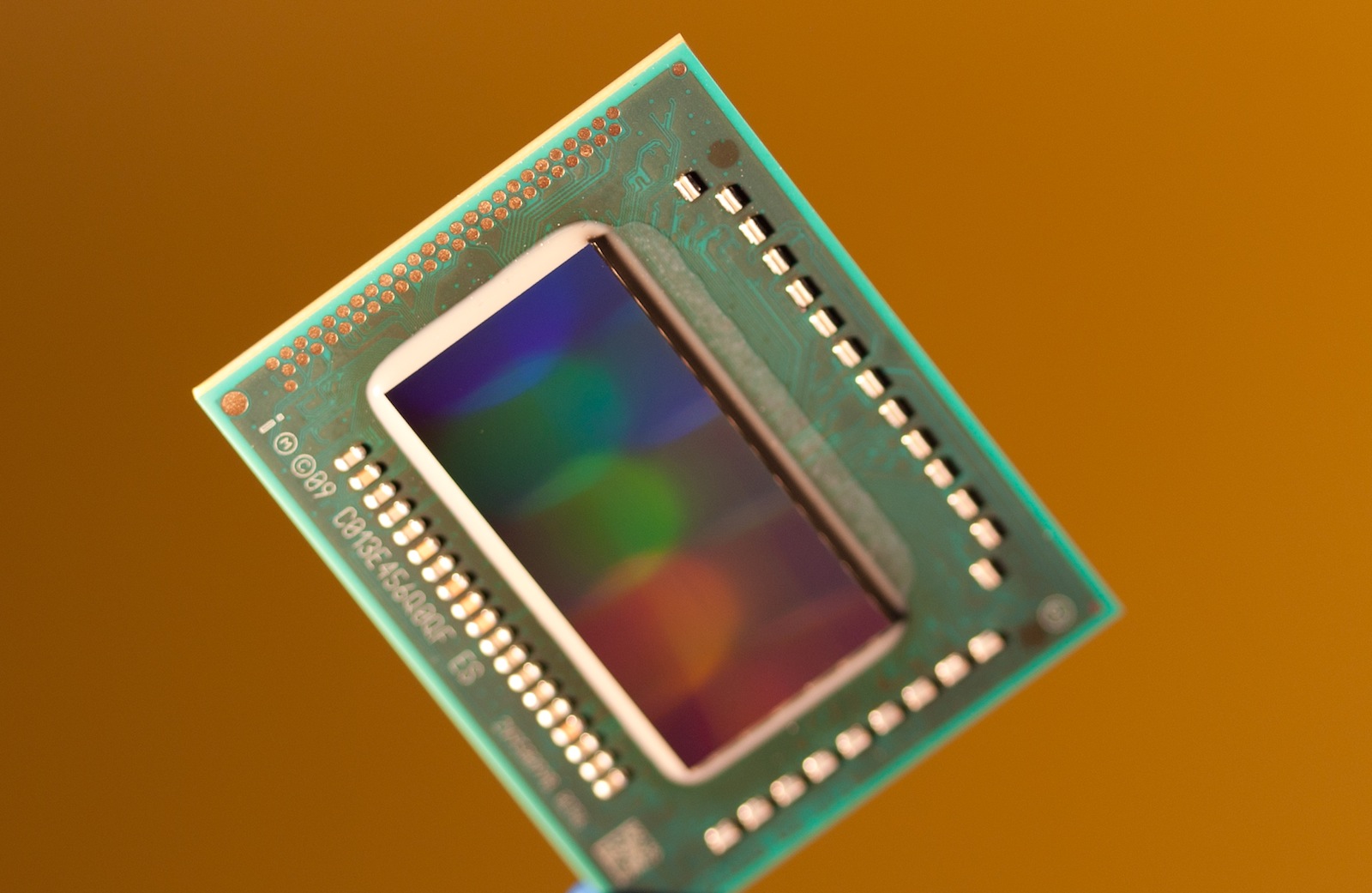
The Intel Core i7-3615QM is a fast quad-core processor for laptops based on the Ivy Bridge architecture. Due to Hyperthreading, the four cores can handle up to eight threads in parallel leading to better utilization of the CPU. Each core offers a base speed of 2.3 GHz but can dynamically increase clock rates with Turbo Boost up to 3.1 GHz (for 4 active cores), 3.2 GHz (for 2 active cores) and 3.3 GHz (for 1 active core).
Ivy Bridge is an enhanced die shrink of the Sandy Bridge architecture with improvements on both GPU and CPU performance. The CPUs are produced in 22nm (versus 32nm Sandy Bridge CPUs) and are the first to introduce 3D transistors for increased energy efficiency when compared to similarly clocked Sandy Bridge processors. Other new features are integrated PCI Express 3.0 and DDR3(L)-1600 support.
The performance of the Core i7-3615QM is slightly above a similarly clocked Sandy Bridge processor due to the architectural improvements. As a result, overall performance is similar to the former fastest model, the Core i7-2920XM.
The integrated Intel HD Graphics 4000 offers 16 Execution Units (EUs) clocked at 650 MHz up to 1200 MHz with Turbo Boost, making it one of the faster variants.
As with most quad-core Ivy Bridge models, the Core i7-3615QM is specified at a TDP of 45 Watts including graphics card and memory controller. Therefore, the CPU is well-suited for laptops 15-inches or greater.
Intel Core i7-1255U
► remove from comparisonThe Intel Core i7-1255U is a high-end mobile CPU for thin and light laptops based on the Alder Lake architecture. It was announced in early 2022 and offers 2 performance cores (P-cores, Golden Cove architecture) and 8 efficient cores (E-cores, Gracemont architecture). The P-cores support Hyper-Threading leading to 12 supported threads when combined with the E-cores. The clock rate ranges from 1.7 to 4.7 GHz on the performance cluster and 1.2 to 3.5 GHz on the efficient cluster. The performance of the E-cores should be similar to old Skylake cores (compare to the Core i7-6700HQ). All cores can use up to 12 MB L3 cache. Compared to the i7-1265U (fastest U-series CPU at launch), the 1255 offers 100 MHz lower clocked CPU cores and only "Essentials" vPro management features. Compared to the P-series (28W) or H-series (45W), the 15W TDP may limit the sustained performance.
Performance
The average 1255U in our database is in the same league as the Ryzen 5 5600U, as far as multi-thread benchmark scores are concerned. Which is nothing to be ashamed of, as of mid 2023.
Thanks to its decent cooling solution and a long-term CPU power limit of 28 W, the Spectre x360 13.5 14t-ef000 is among the fastest laptops built around the 1255U that we know of. It can be 20% faster in CPU-bound workloads than the slowest system featuring the same chip in our database, as of August 2023.
Architecture
The integrated memory controller supports various memory types up to DDR5-4800, DDR4-3200, LPDDR5-5200, and LPDDR4x-4267. The Thread Director (in hardware) can support the operating system to decide which thread to use on the performance or efficient cores for the best performance. For AI tasks, the CPU also integrates GNA 3.0 and DL Boost (via AVX2). Quick Sync in version 8 is the same as in the Rocket Lake CPUs and supports MPEG-2, AVC, VC-1 decode, JPEG, VP8 decode, VP9, HEVC, and AV1 decode in hardware. The CPU only supports PCIe 4.0 (x8 for a GPU and two x4 for SSDs).
The integrated graphics card is based on the Xe-architecture and offers all 96 EUs (Execution Units) operating at up to 1.25 GHz.
Power consumption
This Core i7 has a "minimum assured" power consumption of 12 W. Its Base power consumption sits at 15 W and its maximum Intel-recommended Turbo power consumption isn't supposed to exceed 55 W. All those values are too high to allow for pasisvely cooled designs.
Last but not the least, Core i7-1255U is built with Intel's fourth-gen 10 nm process marketed as Intel 7 for decent, as of late 2022, energy efficiency.
Intel Core i3-1210U
► remove from comparisonThe Intel Core i3-1210U is a low power mobile CPU for thin and light laptops based on the Alder Lake architecture. It was announced in early 2022 and offers 2 performance cores (P-cores, Golden Cove architecture) and 4 efficient cores (E-cores, Gracemont architecture). The P-cores support Hyper-Threading leading to 8 supported threads when combined with the E-cores. The clock rate ranges from 1 to 4.4 GHz on the performance cluster and 0.7 to 3.3 GHz on the efficient cluster. The performance of the E-cores should be similar to old Skylake cores (compare to the Core i7-6700HQ). All cores can use up to 10 MB L3 cache.
Performance
While we have not tested a single system built around the 1210U as of August 2023, we fully expect its multi-thread performance to be pretty much identical to that of the i3-1215U. Which is pretty fast for an entry-level chip, as of mid 2023.
Your mileage may vary depending on how high the CPU power limits are and how competent the cooling solution of your system is.
Features
The integrated memory controller supports various memory types up to DDR5-4800, DDR4-3200, LPDDR5-5200, and LPDDR4x-4267. The Thread Director (in hardware) can support the operating system to decide which thread to use on the performance or efficient cores for the best performance. For AI tasks, the CPU also integrates GNA 3.0 and DL Boost (via AVX2). Quick Sync in version 8 is the same as in the Rocket Lake CPUs and supports MPEG-2, AVC, VC-1 decode, JPEG, VP8 decode, VP9, HEVC, and AV1 decode in hardware. The CPU only supports PCIe 4.0 (x8 for a GPU and two x4 for SSDs).
The integrated graphics adapter is based on the Xe-architecture and offers 64 of the 96 EUs (Execution Units) operating at up to 0.9 GHz.
Power consumption
This Core i3 has a Base power consumption of 9 W, with 29 W being its maximum Intel-recommended Turbo power consumption. TDP values that low allow for passively designs as long as performance is not a priority.
The CPU is built with Intel's 3rd generation 10 nm process marketed as Intel 7 for decent, as of early 2023, energy efficiency.
| Model | Intel Core i7-3615QM | Intel Core i7-1255U | Intel Core i3-1210U | ||||||||||||||||||||||||||||||||||||||||||||||||||||||||||||||||||||||||||||||||||||||||||||||||||||||||||||||||||||||||||||||||||||||||||||||||||||||||||||||||||||||||||||||||||||||||||||
| Codename | Ivy Bridge | Alder Lake-U | Alder Lake-U | ||||||||||||||||||||||||||||||||||||||||||||||||||||||||||||||||||||||||||||||||||||||||||||||||||||||||||||||||||||||||||||||||||||||||||||||||||||||||||||||||||||||||||||||||||||||||||||
| Series | Intel Core i7 | Intel Alder Lake-M | Intel Alder Lake-M | ||||||||||||||||||||||||||||||||||||||||||||||||||||||||||||||||||||||||||||||||||||||||||||||||||||||||||||||||||||||||||||||||||||||||||||||||||||||||||||||||||||||||||||||||||||||||||||
| Series: Alder Lake-M Alder Lake-U |
|
|
| ||||||||||||||||||||||||||||||||||||||||||||||||||||||||||||||||||||||||||||||||||||||||||||||||||||||||||||||||||||||||||||||||||||||||||||||||||||||||||||||||||||||||||||||||||||||||||||
| Clock | 2300 - 3300 MHz | 1200 - 4700 MHz | 700 - 4400 MHz | ||||||||||||||||||||||||||||||||||||||||||||||||||||||||||||||||||||||||||||||||||||||||||||||||||||||||||||||||||||||||||||||||||||||||||||||||||||||||||||||||||||||||||||||||||||||||||||
| L1 Cache | 256 KB | 928 KB | 544 KB | ||||||||||||||||||||||||||||||||||||||||||||||||||||||||||||||||||||||||||||||||||||||||||||||||||||||||||||||||||||||||||||||||||||||||||||||||||||||||||||||||||||||||||||||||||||||||||||
| L2 Cache | 1 MB | 9.5 MB | 5 MB | ||||||||||||||||||||||||||||||||||||||||||||||||||||||||||||||||||||||||||||||||||||||||||||||||||||||||||||||||||||||||||||||||||||||||||||||||||||||||||||||||||||||||||||||||||||||||||||
| L3 Cache | 6 MB | 12 MB | 10 MB | ||||||||||||||||||||||||||||||||||||||||||||||||||||||||||||||||||||||||||||||||||||||||||||||||||||||||||||||||||||||||||||||||||||||||||||||||||||||||||||||||||||||||||||||||||||||||||||
| Cores / Threads | 4 / 8 | 10 / 12 | 6 / 8 | ||||||||||||||||||||||||||||||||||||||||||||||||||||||||||||||||||||||||||||||||||||||||||||||||||||||||||||||||||||||||||||||||||||||||||||||||||||||||||||||||||||||||||||||||||||||||||||
| TDP | 45 Watt | 15 Watt | 9 Watt | ||||||||||||||||||||||||||||||||||||||||||||||||||||||||||||||||||||||||||||||||||||||||||||||||||||||||||||||||||||||||||||||||||||||||||||||||||||||||||||||||||||||||||||||||||||||||||||
| Transistors | 1400 Million | ||||||||||||||||||||||||||||||||||||||||||||||||||||||||||||||||||||||||||||||||||||||||||||||||||||||||||||||||||||||||||||||||||||||||||||||||||||||||||||||||||||||||||||||||||||||||||||||
| Technology | 22 nm | 10 nm | 10 nm | ||||||||||||||||||||||||||||||||||||||||||||||||||||||||||||||||||||||||||||||||||||||||||||||||||||||||||||||||||||||||||||||||||||||||||||||||||||||||||||||||||||||||||||||||||||||||||||
| Die Size | 160 mm2 | ||||||||||||||||||||||||||||||||||||||||||||||||||||||||||||||||||||||||||||||||||||||||||||||||||||||||||||||||||||||||||||||||||||||||||||||||||||||||||||||||||||||||||||||||||||||||||||||
| max. Temp. | 105 °C | 100 °C | 100 °C | ||||||||||||||||||||||||||||||||||||||||||||||||||||||||||||||||||||||||||||||||||||||||||||||||||||||||||||||||||||||||||||||||||||||||||||||||||||||||||||||||||||||||||||||||||||||||||||
| Socket | FCBGA1224, FCPGA988 | BGA1744 | BGA1744 | ||||||||||||||||||||||||||||||||||||||||||||||||||||||||||||||||||||||||||||||||||||||||||||||||||||||||||||||||||||||||||||||||||||||||||||||||||||||||||||||||||||||||||||||||||||||||||||
| Features | HD Graphics 4000 (650-1200MHz), DDR3(L)-1600 Memory Controller, HyperThreading, AVX, Quick Sync, Virtualization | DDR4-3200/LPDDR4x-4266/DDR5-4800/LPDDR5-5200 RAM, PCIe 4, Thr. Dir., DL Boost, GNA, vPro Ess., MMX, SSE, SSE2, SSE3, SSSE3, SSE4.1, SSE4.2, AVX, AVX2, BMI2, ABM, FMA, ADX, SMEP, SMAP, EIST, TM1, TM2, HT, Turbo, SST, AES-NI, RDRAND, RDSEED, SHA | LPDDR4x-4266/LPDDR5-5200 RAM, PCIe 4, Thr. Director, DL Boost, GNA, MMX, SSE, SSE2, SSE3, SSSE3, SSE4.1, SSE4.2, AES, AVX, AVX2, FMA3, SHA | ||||||||||||||||||||||||||||||||||||||||||||||||||||||||||||||||||||||||||||||||||||||||||||||||||||||||||||||||||||||||||||||||||||||||||||||||||||||||||||||||||||||||||||||||||||||||||||
| iGPU | Intel HD Graphics 4000 (650 - 1200 MHz) | Intel Iris Xe Graphics G7 96EUs ( - 1250 MHz) | Intel UHD Graphics 64EUs (Alder Lake 12th Gen) ( - 850 MHz) | ||||||||||||||||||||||||||||||||||||||||||||||||||||||||||||||||||||||||||||||||||||||||||||||||||||||||||||||||||||||||||||||||||||||||||||||||||||||||||||||||||||||||||||||||||||||||||||
| Architecture | x86 | x86 | x86 | ||||||||||||||||||||||||||||||||||||||||||||||||||||||||||||||||||||||||||||||||||||||||||||||||||||||||||||||||||||||||||||||||||||||||||||||||||||||||||||||||||||||||||||||||||||||||||||
| $378 U.S. | |||||||||||||||||||||||||||||||||||||||||||||||||||||||||||||||||||||||||||||||||||||||||||||||||||||||||||||||||||||||||||||||||||||||||||||||||||||||||||||||||||||||||||||||||||||||||||||||
| Announced | |||||||||||||||||||||||||||||||||||||||||||||||||||||||||||||||||||||||||||||||||||||||||||||||||||||||||||||||||||||||||||||||||||||||||||||||||||||||||||||||||||||||||||||||||||||||||||||||
| Manufacturer | ark.intel.com | ark.intel.com | ark.intel.com |

Benchmarks
Average Benchmarks Intel Core i7-3615QM → 0% n=0
Average Benchmarks Intel Core i7-1255U → 0% n=0
* Smaller numbers mean a higher performance
1 This benchmark is not used for the average calculation