 Deutsch
 English
 Español
 Français
 Italiano
 Nederlands
 Polski
 Português
 Русский
 Türkçe
 Svenska
 Chinese
 Magyar
Intel Core 2 Duo T8300 vs Intel Core i5-430M vs Intel Core 2 Duo P7350
Intel Core 2 Duo T8300
► remove from comparisonThe Intel Core 2 Duo T8300 was at the time of announcement a fast dual-core CPU for laptops with 3 MB level 2 cache. It is based on the Penryn core with all features enabled (but without the full 6MB level 2 cache). The later announced Core 2 Duo P7450 was cheaper and used less power.
Intel Core i5-430M
► remove from comparison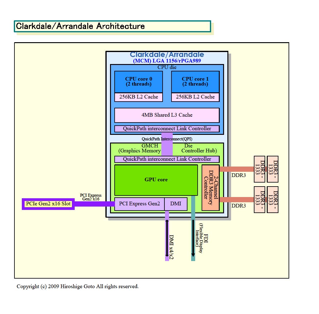
The Intel Core i5-430M is a fast middle class dual core CPU for laptops and clocks (due to the Turbo Mode) from 2.26 to 2.53 GHz. Each core is based on the Nehalem (Westmere) micro-architecture. Hyperthreading enables the Dual Core CPU to handle 4 threads at once (for a better usage of the pipeline). Compared to the faster Core i7-620M, the 430M only has 3 MB Level 3 Cache, missing VT-d, Trusted Execution, and AES features and a lower clock speed.
A feature of the new Core i5-430M is the integrated graphics card (called Intel HD Graphics) and memory controller. Both are on a separate die that is still manufactured in 45nm whereas the CPU die is already manufactured in the new 32nm process.
Due to the integrated memory controller, the HyperThreading and Turbo Boost, the Core i5-430M is faster than a similar clocked Core 2 Duo in all (us known) applications and benchmarks. In fact, the 430M even came close to a fast Core 2 Duo T9600 (2.8 GHz) in some benchmarks (e.g. Cinebench 10 Multi Threaded). This means the 430M is a fast middle class - performance CPU and much faster than the top AMD model, the Turion II Ultra M660 (at the time of announcement).
The 32nm cpu cores of the Westmere generation can also process some new instructions to accelerate AES encryptions. Still, these functions are deactivated on the Core i5-430M leading to some performance drawbacks in modern applications that support AES encoding using the new instructions (e.g. the Communications Suite test in the PCMark Vantage boosts up to 70% using AES in the faster Core i5-520M).
The integrated Intel Graphics Media Accelerator HD (GMA HD) graphics card is between 500-766 MHz (Turbo Boost) and is clearly faster than the old GMA 4500MHD. A GeForce 9400M (ION) should still be a faster (especially as Nvidia and ATI cards have a better driver support than Intel up to now). The Turbo Boost can overclock the Intel HD Graphics up to 733 MHz when the cores are not fully used.
The power consumption of 35 Watt TDP (max.) counts for the whole package and therefore it is clearly better than the 35 Watt TDP of the Core 2 Duo T-series (CPU alone).
Intel Core 2 Duo P7350
► remove from comparisonThe Intel Core 2 Duo P7350 is a dual core processor for laptops. It features 2 GHz and a shared level 2 cache of 3 MB. It is based on the 45nm Penryn core, but Virtualization (VT-x) functions are disabled.
The P7550 uses a Penryn (Montevina Update) core that features 2 integer units, 1 floating point unit, 1 load unit, and 1 store unit in a 14-stages long pipeline. Due to the Wide Dynamic Execution Technology, the core is able to simultaneously execute up to four instructions.
The integrated Enhanced Speedstep is able to downclock the core dynamically as low as 800 MHz to save power (in idle mode).
| Model | Intel Core 2 Duo T8300 | Intel Core i5-430M | Intel Core 2 Duo P7350 | ||||||||||||||||||||||||||||||||||||||||||||||||||||
| Series | Intel Core 2 Duo | Intel Core i5 | Intel Core 2 Duo | ||||||||||||||||||||||||||||||||||||||||||||||||||||
| Codename | Penryn | Arrandale | Penryn | ||||||||||||||||||||||||||||||||||||||||||||||||||||
| Series: Core 2 Duo Penryn |
| ||||||||||||||||||||||||||||||||||||||||||||||||||||||
| Clock | 2400 MHz | 2260 - 2533 MHz | 2000 MHz | ||||||||||||||||||||||||||||||||||||||||||||||||||||
| FSB | 800 | 2500 | 1066 | ||||||||||||||||||||||||||||||||||||||||||||||||||||
| L2 Cache | 3 MB | 512 KB | 3 MB | ||||||||||||||||||||||||||||||||||||||||||||||||||||
| Cores / Threads | 2 / 2 | 2 / 4 | 2 / 2 | ||||||||||||||||||||||||||||||||||||||||||||||||||||
| TDP | 35 Watt | 35 Watt | 25 Watt | ||||||||||||||||||||||||||||||||||||||||||||||||||||
| Transistors | 410 Million | 177 Million | 410 Million | ||||||||||||||||||||||||||||||||||||||||||||||||||||
| 45 nm, 1-1.25V | 32 nm | 45 nm, 1 - 1.25 V | |||||||||||||||||||||||||||||||||||||||||||||||||||||
| Die Size | 107 mm2 | 144 mm2 | 107 mm2 | ||||||||||||||||||||||||||||||||||||||||||||||||||||
| max. Temp. | 105 °C | 105 °C | 90 °C | ||||||||||||||||||||||||||||||||||||||||||||||||||||
| Socket | BGA479, PGA478 | BGA1288, PGA988 | Socket P | ||||||||||||||||||||||||||||||||||||||||||||||||||||
| Features | Virtualization (VT-x), Intel 64, Idle States, Enhanced Speedstep, Execute Disable Bit | Turbo Boost, Hyper Threading, Enhanced Speedstep, integrierte GMA HD 500-733MHz, SSE4.1, SSE4.2 | SSE4.1, Execute Disable Bit, Enhanced Speedstep, Ehnaced Halt State (C1E), 64 Bit, Trusted Execution Technology | ||||||||||||||||||||||||||||||||||||||||||||||||||||
| Architecture | x86 | x86 | x86 | ||||||||||||||||||||||||||||||||||||||||||||||||||||
| $241 U.S. | |||||||||||||||||||||||||||||||||||||||||||||||||||||||
| Announced | |||||||||||||||||||||||||||||||||||||||||||||||||||||||
| Manufacturer | ark.intel.com | ark.intel.com | ark.intel.com | ||||||||||||||||||||||||||||||||||||||||||||||||||||
| L1 Cache | 128 KB | 128 KB | |||||||||||||||||||||||||||||||||||||||||||||||||||||
| L3 Cache | 3 MB |

