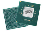
Intel Celeron J4115 vs Intel Core 3 N355 vs Intel Celeron N4100
Intel Celeron J4115
► remove from comparison
The Intel Celeron J4115 is a quad-core SoC primarily for inexpensive mini PCs and was announced late 2017. It runs at 1.8 GHz to 2.5 GHz (Single Core Burst) and is based on the Gemini Lake platform. Similar to the Apollo Lake predecessors, the chip is manufactured on a 14 nm process with FinFETs but offers slightly improved processor cores, double the amount of L2 cache, all in a smaller package. Partial Wi-Fi 5 support is baked into the chip. Besides four CPU cores, the chip also includes a DirectX 12 capable GPU as well as a DDR4/LPDDR4 memory controller (dual-channel, up to 2400 MHz). The processor is not replaceable as it is directly soldered to the mainboard.
Architecture
The processor architecture ist still called Goldmont Plus. Compared to the older Goldmont cores in Apollo Lake, they feature a larger L2 cache (now 4 MB). That means the per-clock-performance should be a bit better, but not anywhere near the Core CPUs like Kaby Lake Y.
Performance
The average J4115 in our database only just matches the Core i5-4260U, a somewhat more power-hungry SoC that saw the light of day in 2014, in multi-thread performance. This means the Celeron is a very basic CPU that isn't really ready to handle anything beyond the most basic tasks such as writing e-mails and listening to Spotify.
Graphics
The UHD Graphics 600 (Gemini Lake) is based on Intel's Generation 9 architecture, which supports DirectX 12 and is also used for the Kaby Lake / Skylake / Apollo Lake graphics adapters (like HD Graphics 520). Equipped with 12 EUs and a clock of up to 750 MHz, the performance should be roughly on par with the older HD Graphics 500 (Apollo Lake).
The chip also includes an advanced video engine with hardware support for the playback of VP9 and H.265 (8-bit color-depth).
Power consumption
Like most other J-class Intel processors, the Celeron has a default TDP (also known as the long-term power limit) of 10 W. This is low enough to allow laptop makers to build passively cooled laptops, mini-PCs, tablets and other gadgetry around the chip.
The Intel Celeron J4115 is built with one of the old 14 nm Intel processes for poor, as of early 2023, energy efficiency.
Intel Core 3 N355
► remove from comparison
The Intel Core 3 N355 (sometimes referred to as the Intel Processor N355) is a mobile processor of the Twin Lake family which is mostly identical to Alder Lake-N, an architecture that will turn 4 in H2 2025. The chip is meant for entry-level laptops, tablets and mini PCs; it offers 8 Efficient (Gracemont) cores that run at up to 3.9 GHz but no Performance cores.
The E-cores do not support Hyper-Threading. No extra threads here.
Performance
The performance of the Core 3 CPU depends heavily on the cooling solution and TDP settings of the system. Provided both are good enough, it will deliver multi-thread benchmark cores on par with older quad-core CPUs like the Ryzen 3 5300U and Core i7-1165G7, which should be enough to run most day-to-day tasks in 2025. Its single-core performance is much less impressive due to the lack of P-cores.
The Alder Lake-N Core i3-N305 (8 cores, up to 3.8 GHz) that was introduced in early 2023 should be just a few percentage points slower than the N355.
Graphics
The SoC comes equipped with a Xe-architecture graphics unit with 32 EUs (Execution Units) running at up to 1.35 GHz. The iGPU can drive up to 3 UHD 2160p monitors and hardware-decodes AV1 among other popular video codecs. Due to the low number of Xe cores and the single-channel RAM restriction, gaming performance is only good enough for older games and fairly low resolutions. GTA V is perfectly playable at 768p on Medium.
Architecture and Features
The integrated memory controller supports single-channel DDR4-3200, DDR5-4800 and LPDDR5-4800 RAM. PCIe NVMe SSD speeds are capped at 3.9 GB/s, corresponding to the PCIe 3 spec. There is no Thunderbolt / USB 4 support here, however, the latest Intel CNVi Wi-Fi 7 wireless networking modules are supported.
Its L3 cache is relatively small at 6 MB, and it has no proper NPU (and thus no Copilot+ branding).
Power consumption
The Intel Core 3 N355 is supposed to consume 15 watts when under longer loads. This is the Intel-recommended PL1 for the chip. While no data on PL2 has been provided, we do know that Asus has given the Core 3 a power limit of 35 watts (PL2) in the NUC 14 Essential.
The SoC is manufactured using the second-generation 10 nm process marketed as Intel 7 meaning power efficiency isn't great here compared to the latest 3 nm silicon from the likes of Apple.
Intel Celeron N4100
► remove from comparison
The Intel Celeron N4100 is a quad-core SoC primarily for inexpensive notebooks and was announced late 2017. It runs at 1.1-2.4 GHz (Single Core Burst, Multi Core Burst max 2.3 GHz) and is based on the Gemini Lake platform. Similar to the Apollo Lake predecessor, the chip is manufactured on a 14 nm process with FinFETs but offers slightly improved processor cores, double the amount of L2 cache, a smaller package, a new generation of monitor outputs (Gen 10) and a partly integrated WiFi chip. Besides four CPU cores, the chip also includes a DirectX 12 capable GPU as well as a DDR4/LPDDR4 memory controller (dual-channel, up to 2400 MHz). The SoC is not replaceable as it is permanently soldered to the mainboard.
Architecture
The processor architecture was slightly reworked and is now called Goldmont Plus. It features an increased Level 2 cache (to 4 MB). That means the per-clock-performance should be a bit better, but not near the Core CPUs like Kaby Lake Y.
Performance
The average N4100 in our database directly competes with AMD's 3020e and 3050e, as far as multi-thread benchmark scores are concerned. The Intel Core m3-8100Y and the Celeron 6305 are close nearby as well. Routinely described as "entry-level" in 2019 and 2020, the Celeron N4100 is a slow processor that is good for the most basic tasks only such as Web browsing with no more than two or three tabs open at a time.
The LapBook Pro is among the fastest systems built around the N4100 that we know of. It can be around 50% faster in CPU-bound workloads than the slowest system featuring the same chip in our database, as of August 2023.
Graphics
The UHD Graphics 600 (Gemini Lake) is based on Intel's Gen9 architecture, which supports DirectX 12 and is also used for the Kaby Lake / Skylake / Apollo Lake graphics adapters (like HD Graphics 520). Equipped with 12 EUs and a clock of up to 700 MHz, the performance should be roughly on par with the older HD Graphics 500 (Apollo Lake).
The chip also includes an advanced video engine with hardware support for the playback of VP9 and H.265 material (8-bit color-depth).
Power Consumption
Celeron N4100 has a default TDP of 6 W (also known as PL1), making it a great option for passively cooled setups.
The fairly old 14 nm process this Celeron is built with makes for so-so, as of mid-2022, energy efficiency.
| Model | Intel Celeron J4115 | Intel Core 3 N355 | Intel Celeron N4100 | ||||||||||||||||||||||||||||||||||||||||||||||||||||||||||||||||
| Codename | Gemini Lake | Twin Lake | Gemini Lake | ||||||||||||||||||||||||||||||||||||||||||||||||||||||||||||||||
| Series | Intel Gemini Lake | Intel Alder Lake-N | Intel Gemini Lake | ||||||||||||||||||||||||||||||||||||||||||||||||||||||||||||||||
| Series: Gemini Lake Gemini Lake |
|
|
| ||||||||||||||||||||||||||||||||||||||||||||||||||||||||||||||||
| Clock | 1800 - 2500 MHz | 3000 - 3900 MHz | 1100 - 2400 MHz | ||||||||||||||||||||||||||||||||||||||||||||||||||||||||||||||||
| L2 Cache | 4 MB | 4 MB | 4 MB | ||||||||||||||||||||||||||||||||||||||||||||||||||||||||||||||||
| Cores / Threads | 4 / 4 | 8 / 8 8 x 3.9 GHz Intel Gracemont E-Core | 4 / 4 | ||||||||||||||||||||||||||||||||||||||||||||||||||||||||||||||||
| TDP | 10 Watt | 15 Watt | 6 Watt | ||||||||||||||||||||||||||||||||||||||||||||||||||||||||||||||||
| Technology | 14 nm | 10 nm | 14 nm | ||||||||||||||||||||||||||||||||||||||||||||||||||||||||||||||||
| max. Temp. | 105 °C | 105 °C | |||||||||||||||||||||||||||||||||||||||||||||||||||||||||||||||||
| Socket | BGA1090 | BGA1264 | BGA1090 | ||||||||||||||||||||||||||||||||||||||||||||||||||||||||||||||||
| Features | DDR4-2400/LPDDR4-2400 RAM, PCIe 2, MMX, SSE, SSE2, SSE3, SSSE3, SSE4.1, SSE4.2, VMX, SMEP, SMAP, MPX, EIST, TM1, TM2, Turbo, AES-NI, RDRAND, RDSEED, SHA, SGX | DDR4-3200/DDR5-4800/LPDDR5-4800 RAM (sin. chan.), PCIe 3, GNA, MMX, SSE, SSE2, SSE3, SSSE3, SSE4.1, SSE4.2, AVX, AVX2, BMI2, ABM, FMA, ADX, VMX, SMEP, SMAP, EIST, TM1, TM2, Turbo, SST, AES-NI, RDRAND, RDSEED, SHA | DDR4-2400/LPDDR4-2400 RAM, PCIe 2, MMX, SSE, SSE2, SSE3, SSSE3, SSE4.1, SSE4.2, VMX, SMEP, SMAP, MPX, EIST, TM1, TM2, Turbo, AES-NI, RDRAND, RDSEED, SHA, SGX | ||||||||||||||||||||||||||||||||||||||||||||||||||||||||||||||||
| iGPU | Intel UHD Graphics 600 (250 - 750 MHz) | Intel UHD Graphics 32EUs (Alder Lake) ( - 1350 MHz) | Intel UHD Graphics 600 (200 - 700 MHz) | ||||||||||||||||||||||||||||||||||||||||||||||||||||||||||||||||
| Architecture | x86 | x86 | x86 | ||||||||||||||||||||||||||||||||||||||||||||||||||||||||||||||||
| Announced | |||||||||||||||||||||||||||||||||||||||||||||||||||||||||||||||||||
| Manufacturer | ark.intel.com | www.intel.com | ark.intel.com | ||||||||||||||||||||||||||||||||||||||||||||||||||||||||||||||||
| L1 Cache | 768 KB | ||||||||||||||||||||||||||||||||||||||||||||||||||||||||||||||||||
| L3 Cache | 6 MB | ||||||||||||||||||||||||||||||||||||||||||||||||||||||||||||||||||
| $107 U.S. |
Benchmarks
Average Benchmarks Intel Celeron J4115 → 100% n=34
Average Benchmarks Intel Core 3 N355 → 291% n=34
Average Benchmarks Intel Celeron N4100 → 85% n=34
* Smaller numbers mean a higher performance
1 This benchmark is not used for the average calculation


