

AMD Ryzen 7 5800U vs Intel Core i5-1155G7 vs Intel Core i5-1145G7
AMD Ryzen 7 5800U
► remove from comparison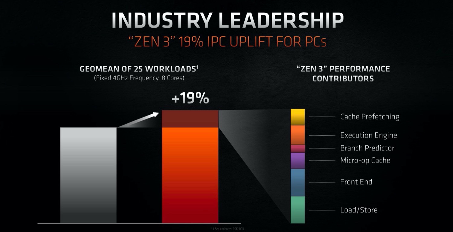
The AMD Ryzen 7 5800U is a processor for thin and light laptops based on the Cezanne generation. The R7 5800U integrates all eight cores based on the Zen 3 microarchitecture and is the fastest U-series processor at launch. They are clocked at 1.9 (guaranteed base clock) to 4.4 GHz (Turbo) and support SMT / Hyperthreading (16 threads). The chip is manufactured on the modern 7 nm TSMC process.
The new Zen 3 microarchitecture offers a significantly higher IPC (instructions per clock) compared to Zen 2. For desktop processors AMD claims 19 percent on average and in applications reviews showed around 12% gains at the same clock speed.
In addition to the eight CPU cores, the APU also integrates a Radeon RX Vega 8 GPU with 8 CUs at up to 2000 MHz. The dual channel memory controller supports DDR4-3200 and energy efficient LPDDR4-4266 RAM. Furthermore, 16 MB level 3 cache (up from 8 MB at the 4800U) can be found on the chip.
Performance
The average 5800U in our database matches the Core i5-11260H and, perhaps a little disappointingly, the Ryzen 7 4800U in multi-core performance.
Thanks to its decent cooling solution and a long-term CPU power limit of 22 W, the ProBook x360 435 G8 is among the fastest laptops powered by the 5800U that we know of. It can be more than 10% faster in CPU-bound workloads than the slowest system featuring the same chip in our database, as of August 2023.
Power consumption
This Ryzen 7 series chip has a default TDP (also known as the long-term power limit) of 15 W, a value that laptop makers are allowed to change to anything between 10 W and 25 W with clock speeds and performance changing accordingly as a result. Choosing the lowest value would allow one to build a passively cooled system around the Ryzen, however, most laptop manufacturers will do the opposite to extract as much performance out of the chip as possible.
The Ryzen 7 5800U is built with TSMC's 7 nm process for average, as of mid 2023, energy efficiency.
Intel Core i5-1155G7
► remove from comparison
The Intel Core i5-1155G7 is a power efficient quad-core SoC for laptops and Ultrabooks based on the Tiger Lake-U generation that was announced in mid 2021 as part of the refresh. It integrates four Willow Cove processor cores (8 threads thanks to HyperThreading). The base clock speed depends on the TDP settings and ranges from 1 GHz (12 Watt TDP) up to 2.5 GHz (28 Watt). Boost clock speed is 4.5 GHz.
Tiger Lake SoCs add PCIe 4 support (4 lanes), AI hardware acceleration, and the partial integration of Thunderbolt 4 / USB 4 and Wifi 6 in the chip.
Another novelty is the integrated Xe graphics adapter with 80 EUs based on the completely new Gen 12 architecture. It offers a significantly higher performance compared to the older Iris Plus G7 (Ice Lake).
Performance
The average 1155G7 in our database proves to be a very decent mid-range processor, as of mid 2022, trading blows with the Core i7-10810U and the Ryzen 5 4500U as far as multi-thread benchmark scores are concerned. While perhaps not the best option for power users, this Core i5 will make most consumers happy, providing for short load times and generally pain-free experience.
Your mileage may vary depending on how high the CPU power limits are and how competent the cooling solution of your system is.
Power consumption
This Core i5 series chip has a default TDP, also known as the long-term power limit, of 12 W to 28 W, the expectation being that laptop makers will go for a higher value in exchange for higher performance. Either way, this is a tad too high to allow for passively cooled designs.
The i5-1155G7 is built with Intel's third-gen 10 nm process marketed as SuperFin for lower-than-average, as of early 2023, energy efficiency.
Intel Core i5-1145G7
► remove from comparisonThe Intel Core i5-1145G7 is a power efficient quad-core SoC for laptops and Ultrabooks based on the Tiger Lake-U generation that was announced early 2021. It integrates four Willow Cove processor cores (8 threads thanks to HyperThreading). The base clock speed depends on the TDP settings and ranges from 1.1 GHz (12 Watt TDP) up to 2.6 GHz (28 Watt). The Boost is always specified at 4.4 GHz (one or two cores).
Another novelty is the integrated Xe graphics card with 80 EUs based on the completely new Gen 12 architecture. It offers a significantly higher performance compared to the older Iris Plus G7 (Ice Lake).
Furthermore, Tiger Lake SoCs add PCIe 4 support (4 lanes), AI hardware acceleration, and the partial integration of Thunderbolt 4 / USB 4 and Wifi 6 in the chip. In addition to this, the i5 supports vPro for easy remote management.
The chip is produced on the improved 10nm SuperFin process at Intel that should be comparable to the 7nm process at TSMC (e.g. Ryzen 4000 series).
All articles on Tiger Lake can be found on our Tiger Lake architecture hub.
| Model | AMD Ryzen 7 5800U | Intel Core i5-1155G7 | Intel Core i5-1145G7 | ||||||||||||||||||||||||||||||||||||||||||||||||||||||||||||||||||||||||||||||||
| Codename | Cezanne-U (Zen 3) | Tiger Lake-UP3 | Tiger Lake-UP3 | ||||||||||||||||||||||||||||||||||||||||||||||||||||||||||||||||||||||||||||||||
| Series | AMD Cezanne (Zen 3, Ryzen 5000) | Intel Tiger Lake | Intel Tiger Lake | ||||||||||||||||||||||||||||||||||||||||||||||||||||||||||||||||||||||||||||||||
| Series: Tiger Lake Tiger Lake-UP3 |
|
|
| ||||||||||||||||||||||||||||||||||||||||||||||||||||||||||||||||||||||||||||||||
| Clock | 1900 - 4400 MHz | 2500 - 4500 MHz | 2600 - 4400 MHz | ||||||||||||||||||||||||||||||||||||||||||||||||||||||||||||||||||||||||||||||||
| L1 Cache | 512 KB | 320 KB | 320 KB | ||||||||||||||||||||||||||||||||||||||||||||||||||||||||||||||||||||||||||||||||
| L2 Cache | 4 MB | 5 MB | 5 MB | ||||||||||||||||||||||||||||||||||||||||||||||||||||||||||||||||||||||||||||||||
| L3 Cache | 16 MB | 8 MB | 8 MB | ||||||||||||||||||||||||||||||||||||||||||||||||||||||||||||||||||||||||||||||||
| Cores / Threads | 8 / 16 | 4 / 8 | 4 / 8 | ||||||||||||||||||||||||||||||||||||||||||||||||||||||||||||||||||||||||||||||||
| TDP | 25 Watt | 28 Watt | 28 Watt | ||||||||||||||||||||||||||||||||||||||||||||||||||||||||||||||||||||||||||||||||
| Technology | 7 nm | 10 nm | 10 nm | ||||||||||||||||||||||||||||||||||||||||||||||||||||||||||||||||||||||||||||||||
| max. Temp. | 105 °C | 100 °C | 100 °C | ||||||||||||||||||||||||||||||||||||||||||||||||||||||||||||||||||||||||||||||||
| Socket | FP6 | BGA1449 | BGA1449 | ||||||||||||||||||||||||||||||||||||||||||||||||||||||||||||||||||||||||||||||||
| Features | DDR4-3200/LPDDR4-4266 RAM, PCIe 3, MMX, SSE, SSE2, SSE3, SSSE3, SSE4A, SSE4.1, SSE4.2, AVX, AVX2, BMI2, ABM, FMA, ADX, SMEP, SMAP, SMT, CPB, AES-NI, RDRAND, RDSEED, SHA, SME | DDR4-3200/LPDDR4x-4266 RAM, PCIe 4, 4 GT/s bus, DL Boost, GNA, MMX, SSE, SSE2, SSE3, SSSE3, SSE4.1, SSE4.2, AVX, AVX2, AVX-512, BMI2, ABM, FMA, ADX, VMX, SMEP, SMAP, EIST, TM1, TM2, HT, Turbo, SST, AES-NI, RDRAND, RDSEED, SHA | DDR4-3200/LPDDR4x-4266 RAM, PCIe 4, 4 GT/s bus, DL Boost, GNA, vPro, MMX, SSE, SSE2, SSE3, SSSE3, SSE4.1, SSE4.2, AVX, AVX2, AVX-512, BMI2, ABM, FMA, ADX, VMX, SMX, SMEP, SMAP, EIST, TM1, TM2, HT, Turbo, SST, AES-NI, RDRAND, RDSEED, SHA, TME | ||||||||||||||||||||||||||||||||||||||||||||||||||||||||||||||||||||||||||||||||
| iGPU | AMD Radeon RX Vega 8 (Ryzen 4000/5000) ( - 2000 MHz) | Intel Iris Xe Graphics G7 80EUs (400 - 1350 MHz) | Intel Iris Xe Graphics G7 80EUs (400 - 1300 MHz) | ||||||||||||||||||||||||||||||||||||||||||||||||||||||||||||||||||||||||||||||||
| Architecture | x86 | x86 | x86 | ||||||||||||||||||||||||||||||||||||||||||||||||||||||||||||||||||||||||||||||||
| Announced | |||||||||||||||||||||||||||||||||||||||||||||||||||||||||||||||||||||||||||||||||||
| Manufacturer | www.amd.com | ark.intel.com | ark.intel.com |

Benchmarks

Average Benchmarks AMD Ryzen 7 5800U → 100% n=22
Average Benchmarks Intel Core i5-1155G7 → 85% n=22
Average Benchmarks Intel Core i5-1145G7 → 79% n=22
* Smaller numbers mean a higher performance
1 This benchmark is not used for the average calculation