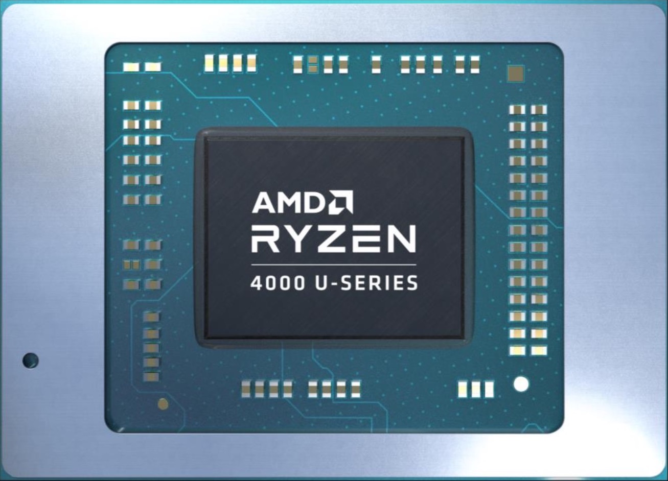
The AMD Ryzen 7 4700U is a processor for thin and light laptops based on the Renoir architecture. The 4700U integrates all eight cores based on the Zen 2 microarchitecture. They are clocked at 2 (guaranteed base clock) to 4.1 GHz (Turbo). There is no support for the thread-doubling SMT tech. The chip is manufactured on the modern 7 nm TSMC process and partly thanks to it AMD advertises a 2x improved performance per Watt for the Renoir chips. Compared to the faster R7 4800U, the 4700U offers slightly lower clock speeds and no support for SMT / Hyperthreading.
In addition to the eight CPU cores, the APU also integrates a Radeon RX Vega 7 integrated graphics card with 7 CUs and up to 1600 MHz. The dual channel memory controller supports DDR4-3200 and energy efficient LPDDR4-4266 RAM. Furthermore, 8 MB level 3 cache can be found on the chip. See our hub page on the Renoir Processors for more information.
Performance
The average 4700U in our database proves to be a rather competent little processor. It trades blows with the much more power-hungry Intel Core i7-10750H, as far as multi-thread benchmark scores are concerned. While it fails to get far enough away from the more affordable Ryzen 5 4600U, this Ryzen 7 is still a good CPU for most tasks.
Your mileage may vary depending on how competent the cooling solution of your laptop is and how high the CPU power limits are.
Power consumption
The Ryzen 7 4700U is a 15 W chip. However, laptop makers are allowed to change that value to anything between 10 W and 25 W, with clock speeds and long-term performance changing accordingly as a result. By going for the lowest value, it is possible to build a passively cooled system around the APU.
The fairly modern 7 nm TSMC process this Ryzen is manufactured on makes for above average, as of mid 2022, energy efficiency.
The Intel Core i5-5300U is an ULV (ultra low voltage) dual-core processor based on the Broadwell architecture, which has been launched in January 2015. In addition to two CPU cores with Hyper-Threading clocked at 2.3 - 2.9 GHz (2 Cores: 2.7 GHz), the chip also integrates an HD Graphics 5500 GPU and a dual-channel DDR3(L)-1600 memory controller. The Core i5 is manufactured in a 14 nm process with FinFET transistors.
Compared to the Core i5-5350U, the i5-5300U features a higher CPU base clock, but integrates a somewhat slower GPU.
Architecture
Broadwell represents the "Tick" in Intel's Tick-Tock model, which means a shrink of its predecessor Haswell. The new 14 nm manufacturing process with three-dimensional FinFET transistors allows not only improvements in energy efficiency, but also a significantly smaller die size fit for more compact packages and devices.
Further advantages result from the revised microarchitecture of Broadwell. Due to its improved branch prediction, bigger buffer sizes (1500 instead of 1000 entries in the L2 TLB) and other tweaks, the performance per clock has been increased by more than 5 percent over its predecessor. There are also some new instruction set extensions designed for cryptographic applications.
Performance
Thanks to its improved architecture, the Core i5-5300U ends up 5 - 15 percent faster than the slightly lower clocked Core i5-4300U and beats the Core i7-4510U (both Haswell). Thus, the CPU has sufficient power for office and multimedia purposes as well as more demanding applications and multitasking.
Graphics
The integrated HD Graphics 5500 offers 24 Execution Units (EUs) clocked at 300 - 900 MHz. Similar to the CPU core, the GPU architecture (Intel Gen 8) has been thoroughly revised for improved performance-per-clock. Therefore, the HD Graphics 5500 is able to outperform the HD Graphics 4400 (20 EUs) as well as the HD Graphics 5000 (40 EUs), both part of the Haswell generation. Nevertheless, most games as of 2015 will be playable only in low settings.
Broadwell is the first Intel chip to fully support DirectX 11.2 as well as OpenCL 1.3/2.0 and OpenGL 4.3. Video will output natively via DisplayPort 1.2 or HDMI 1.4a. However, the new HDMI 2.0 standard is not supported.
Power Consumption
The i5-5300U is rated at a TDP of 15 W (7.5 W cTDP Down) including the graphics card, memory controller, VRMs and the integrated chipset. Therefore, the CPU is suited even for small ultrabooks 11-inches and greater.
The Intel Core i5-5287U is a fast dual-core processor based on the Broadwell architecture, which has been launched in January 2015. With a TDP of 28 W, the CPU is suited for medium-sized ultrabooks and notebooks, whereas smaller devices will use more power efficient ULV models such as the Core i5-5200U (15 W TDP). In addition to two CPU cores with Hyper-Threading clocked at 2.9 - 3.3 GHz (2 Cores: 3.3 GHz as well), the chip also integrates an Iris Graphics 6100 GPU and a dual-channel LPDDR3-1866/DDR3L-1600 memory controller. The Core i5 is manufactured in a 14 nm process with FinFET transistors.
Architecture
Broadwell represents the "Tick" in Intel's Tick-Tock model, which means a shrink of its predecessor Haswell. The new 14 nm manufacturing process with three-dimensional FinFET transistors allows not only improvements in energy efficiency, but also a significantly smaller die size fit for more compact packages and devices.
Further advantages result from the revised microarchitecture of Broadwell. Due to its improved branch prediction, bigger buffer sizes (1500 instead of 1000 entries in the L2 TLB) and other tweaks, the performance per clock has been increased by more than 5 percent over its predecessor. There are also some new instruction set extensions designed for cryptographic applications.
Performance
Thanks to its improved architecture, the Core i5-5287U almost matches the slightly higher clocked predecessor Core i7-4578U (Haswell, 28 W). Thus, the CPU has sufficient power even for demanding applications and multitasking.
Graphics
The integrated Iris Graphics 6100 offers 48 Execution Units (EUs) clocked at 300 - 1100 MHz. Similar to the CPU core, the GPU architecture (Intel Gen 8) has been thoroughly revised for improved performance-per-clock. In addition, the GPU benefits from faster memory speeds up to LPDDR3-1866 (Haswell: DDR3-1600). We expect the Iris Graphics 6100 to be significantly faster than the former Iris Graphics 5100. Nevertheless, demanding games as of 2015 should be playable only in low or medium settings.
Broadwell is the first Intel chip to fully support DirectX 11.2 as well as OpenCL 1.3/2.0 and OpenGL 4.3. Video will output natively via DisplayPort 1.2 or HDMI 1.4a. However, the new HDMI 2.0 standard is not officially supported.
Power Consumption
The i5-5287U is rated at a TDP of 28 W including the graphics card, memory controller, VRMs and the integrated chipset. Therefore, the CPU is suited for medium-sized ultrabooks 13-inches or greater.
- Range of benchmark values for this graphics card - Average benchmark values for this graphics card * Smaller numbers mean a higher performance 1 This benchmark is not used for the average calculation
v1.34
log 05. 14:39:49
#0 ran 0s before starting gpusingle class +0s ... 0s
#1 checking url part for id 11683 +0s ... 0s
#2 checking url part for id 6385 +0s ... 0s
#3 checking url part for id 6405 +0s ... 0s
#4 redirected to Ajax server, took 1759667989s time from redirect:0 +0s ... 0s
#5 did not recreate cache, as it is less than 5 days old! Created at Sat, 04 Oct 2025 05:18:30 +0200 +0s ... 0s
#6 composed specs +0.009s ... 0.009s
#7 did output specs +0s ... 0.009s
#8 getting avg benchmarks for device 11683 +0.004s ... 0.013s
#9 got single benchmarks 11683 +0.018s ... 0.031s
#10 getting avg benchmarks for device 6385 +0.001s ... 0.031s
#11 got single benchmarks 6385 +0.01s ... 0.041s
#12 getting avg benchmarks for device 6405 +0s ... 0.042s
#13 got single benchmarks 6405 +0s ... 0.042s
#14 got avg benchmarks for devices +0s ... 0.042s
#15 min, max, avg, median took s +0.049s ... 0.091s