 Deutsch
 English
 Español
 Français
 Italiano
 Nederlands
 Polski
 Português
 Русский
 Türkçe
 Svenska
 Chinese
 Magyar
Intel HD Graphics P630 vs Intel UHD Graphics (Jasper Lake 24 EU)
Intel HD Graphics P630
► remove from comparison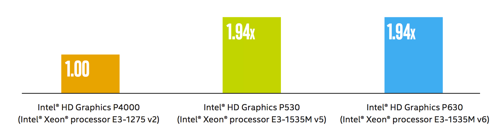
The Intel HD Graphics P630 (GT2) is an integrated graphics unit, which can be found in various Xeon workstation processors of the Kaby Lake generation. The "GT2" version of the Skylake GPU offers 24 Execution Units (EUs) clocked at up to 1050 MHz (depending on the CPU model). Due to its lack of dedicated graphics memory or eDRAM cache, the P630 has to access the main memory (2x 64bit DDR3L-1600 / DDR4-2133). It uses the same silicon as the consumer HD Graphics 630 in Kaby-Lake-H processors but features optimized drivers for workstaion and CAD software. According to Intel it is certified for 15 applications (see list).
Performance
According to Intel, the performance of the P630 is identical to the Intel HD Graphis P530 (Skylake predecessor) processor graphics card and 1.94x faster than the old Intel HD Graphics P4000. Compared to consumer cards, the gaming performance should be on a similar level to the dedicated GeForce 920M and will handle old games (as of 2015) in low or medium settings.
Features
The revised video engine in the Kaby Lake chips now supports H.265/HEVC Main10 profile at 10-bit color depth and also the VP9 codec in hardware. Furthermore, HDCP 2.2 is also supported in all chips, which allows Netflix 4K videos, for instance.
Power Consumption
The HD Graphics P630 can be found in mobile quad-core Xeon processors with 45 W TDP and also desktop processors of the Xeon range with higher TDPs.
Source: http://www.intel.com/content/dam/www/public/us/en/documents/guides/hd-graphics-performance-guide.pdf
Intel UHD Graphics (Jasper Lake 24 EU)
► remove from comparison
The Intel UHD Graphics 24 EUs (Jasper Lake, Gen. 11) is an integrated graphics card in the Jasper Lake Celeron SoCs for laptops and small desktops. It is the mid range GPU version in the Jasper Lake series (Celeron Quad-Cores) and offers 24 of the 32 EUs (Execution Units / Shader Blocks). It offers no dedicated graphics memory and the clock rate depends on the processor model. At launch there are two Celeron models (N5100 with 6W and N5105 with 10W) clocked at 350 - 800 MHz.
Thanks to the improved architecture and more EUs, the UHD Graphics is clearly faster than the old Gemini Lake SoCs (e.g. N5000).
A special new feature of the Gen11 graphics card is the new Variable Rate Shading (VRS) support. With it game designers can decide where to spend shading time and e.g. shade object in the background or behind fog with less resolution (up to using only one source for a 4x4 block). With this technique early results show up to 1.3x performance in Unreal Engine POC and 1.2x speedup in Civ 6. Up to now VRS is only supported by the new Nvidia Turing architecture (GTX 1650 and up).
Another improved hardware piece is the integrated video de- and encoder that was improved significantly according to Intel. They did not specify any more details, but the previous generation was able to decode VP9 and H.265/HEVC in Main10 profile with 10 bit color depth using the dedicated hardware.
The Jasper Lake SoCs and therefore the integrated GPU are manufactured in the 10nm process (like Ice Lake probably) at Intel that should be comparable to the 7nm process of TSMC.
| Intel HD Graphics P630 | Intel UHD Graphics (Jasper Lake 24 EU) | ||||||||||||||||||||||||||||||||||||||||||||||||||||||||||||||||||||||
| Gen. 11 Series |
|
| |||||||||||||||||||||||||||||||||||||||||||||||||||||||||||||||||||||
| Codename | Kaby-Lake-H-GT2 | Gen. 11 | |||||||||||||||||||||||||||||||||||||||||||||||||||||||||||||||||||||
| Architecture | Gen. 9.5 Kaby Lake | Gen. 11 | |||||||||||||||||||||||||||||||||||||||||||||||||||||||||||||||||||||
| Pipelines | 24 - unified | 24 - unified | |||||||||||||||||||||||||||||||||||||||||||||||||||||||||||||||||||||
| Memory Bus Width | 64/128 Bit | ||||||||||||||||||||||||||||||||||||||||||||||||||||||||||||||||||||||
| Shared Memory | yes | yes | |||||||||||||||||||||||||||||||||||||||||||||||||||||||||||||||||||||
| API | DirectX 12_1, OpenGL 4.4 | DirectX 12_1, OpenGL 4.5 | |||||||||||||||||||||||||||||||||||||||||||||||||||||||||||||||||||||
| technology | 14 nm | 10 nm | |||||||||||||||||||||||||||||||||||||||||||||||||||||||||||||||||||||
| Features | QuickSync | QuickSync | |||||||||||||||||||||||||||||||||||||||||||||||||||||||||||||||||||||
| Date of Announcement | 05.08.2015 | 11.01.2021 | |||||||||||||||||||||||||||||||||||||||||||||||||||||||||||||||||||||
| Core Speed | 350 - 800 (Boost) MHz | ||||||||||||||||||||||||||||||||||||||||||||||||||||||||||||||||||||||
| Power Consumption | 4.8 - 10 Watt |
|
| ||||||||||||||||||||||||||||||||


