 Deutsch
 English
 Español
 Français
 Italiano
 Nederlands
 Polski
 Português
 Русский
 Türkçe
 Svenska
 Chinese
 Magyar
Intel Celeron N3350 vs AMD A9-9420e vs Intel Celeron J3355
Intel Celeron N3350
► remove from comparisonThe Intel Celeron N3350 is an Apollo Lake family, dual-core, ultra-low-power processor (SoC) that saw the light of day in 2016. Its two cores run at 1.1 GHz to 2.4 GHz; these are not Hyper-Threading-enabled meaning there are no additional threads. This chip has a fairly competent integrated graphics solution, the Intel HD Graphics 500, and eats very little (~6 W).
Amusingly enough, Intel keeps making and selling the Celeron as of late 2022, albeit the price has dropped from about $100 to about $20 per unit making the CPU even more popular with ultra-budget nettop and laptop makers.
Architecture & Features
Just like other Celeron N, Celeron J, Pentium N, Pentium J processors, this Celeron is notable for its small die size. It is easy to manufacture, lowering the costs and enabling Intel to compete with various ARM-based products (hello, Raspberry Pi).
The Celeron N3350 features the Goldmont CPU microarchitecture. This replaces the dated Silvermont (2013), bringing with it several welcome improvements and making for a double-digit IPC improvement. There is still no L3 cache to be found here, however, it now takes less cycles to perform many operations.
The Celeron is compatible with DDR3L-1866, LPDDR3-1866, LPDDR4-2400 RAM. Intel's guidelines state that up to 8 GB are supported; that being said, various forum users report that the CPU functions just fine if mated to 16 GB and even 32 GB of RAM. The chip features six PCI-Express 2.0 lanes for connecting various devices, meaning a four-lane NVMe SSD will not be able to deliver a data transfer rate of more than 2 GB/s. eMMC and SATA storage is supported natively, too.
This Intel CPU is Secure Boot-compatible; technically, it will have no issue running 64-bit Windows 11. However, Microsoft only allows Windows 11 to be installed on systems with CPUs released in 2017 or later, making 64-bit Windows 10 the only OS that the Celeron is officially compatible with.
Last but not the least, please keep in mind that this is not a user-replaceable CPU. It gets permanently soldered to the motherboard (BGA1296 socket interface).
Performance
The average N3350 in our database is just as fast as the Atom x5-Z8300 and the Core 2 Duo SU7300, as far as multi-thread benchmark scores are concerned. Which is not fast at all. In fact, the two cores of this Celeron trail behind a single core of any half-decent CPU such as Intel's very own Core i3-7130U. A proper x86 CPU, Celeron N3350 will let you run nearly any Windows app, the caveat being that you will have to wait for several seconds every time you click on something. Windows 10 takes nearly a minute to fully boot with this CPU.
Graphics
The Intel HD Graphics 500 (Apollo Lake) is the highlight of this little Celeron. As far as the feature set is concerned, the HD Graphics 500 is not much different from the HD Graphics 520 or any other graphics adapter that full-blown six-generation Intel Core i3/i5/i7 chips have. This iGPU is compatible with DX12; it will drive up to 3 monitors with resolutions as high as 2160p60. It will happily decode VP9 and AVC-encoded videos, too. These are the two codecs that YouTube mostly relies on, as of 2021.
It's not all roses and sunshine. To keep power consumption under control, the number of Execution Units was reduced to 12 (the HD Graphics 520 has 24 EUs at its disposal, for reference). Besides, the UHD Graphics runs at up to 650 MHz which is not a lot. Very few games will be playable on this graphics solution - mostly, ones that were released in the 2000s or even in the 1990s.
Power consumption
The Celeron's default TDP (also known as the Power Limit 1) is 6 W, making it a great option for passively cooled systems. Increasing the PL1 by one or two watts, which many systems built around Apollo Lake allow one to do, makes for a much more responsive user experience, speaking subjectively.
Energy efficiency isn't great here, as Intel's 14 nm processes are very old as of mid 2022.
AMD A9-9420e
► remove from comparison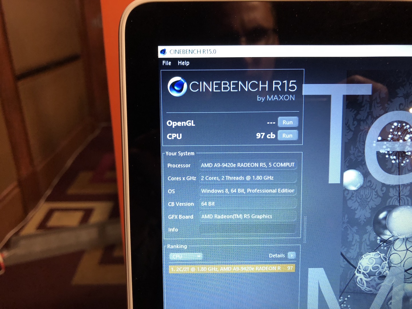
The AMD A9-9420e is an entry-level chip from the Stoney-Ridge APU series for notebooks (7th APU generation). It was first found in the Dell Inspiron 3000 with passive cooling and 4 GB DDR4 RAM. The performance in that device was way below the normal A9-9420 as the clock speed only reached up to 2,5 GHz. It also includes a Radeon R5 GPU with 192 shaders as well as a single-channel DDR4-2133 memory controller, H.265 video engine and chipset with all I/O ports.
Architecture
Stoney Ridge is the successor of the Carrizo architecture and the design is almost identical. Thanks to optimized manufacturing processes and more aggressive Boost behavior, however, the clocks are a bit higher at the same power consumption. The memory controller now also supports DDR4-RAM, in this case up to 2133 MHz. Stoney Ridge is the designation for the smaller dual-core and single-core chip, while Bristol Ridge is the bigger quad-core chip with dual-channel memory controller. More technical details are available in the following articles:
Power Consumption
AMD specifies the TDP of the A9-9420 between 10-25 Watts, but the passively cooled A9-9420e should be positioned lower than 9 Watt.
Intel Celeron J3355
► remove from comparisonThe Intel Celeron J3355 is a dual-core SoC primarily for inexpensive notebooks and was announced in late 2016. It runs at 2 - 2.5 GHz (Single Core Burst) and is based on the Apollo Lake platform. Similar to the Braswell predecessor, the chip is manufactured in a 14 nm process (P1273) with FinFETs. Besides two CPU cores, the chip also includes a DirectX 12 capable GPU as well as a DDR3L/LPDDR3/LPDDR4 memory controller (dual-channel, up to 1866/2400 MHz).
Architecture
For the first time in a couple of years, Intel completely reworked the CPU architecture of the Atom series. The manufacturer advertises performance gains of roughly 30 percent, but does not reveal any specifics about the individual changes. The new Goldmont architecture should therefore be roughly on par with AMD's Beema/Carrizo-L APUs in terms of per-MHz performance, but it still far behind the more expensive Core CPUs (like Skylake / Kaby Lake).
Performance
The CPU performance of the Celeron J3355 is slightly better than the lower power Celeron N3350 and less depending on the cooling solution. This means the processor is only suited for light daily tasks (office, browsing).
GPU Performance
The HD Graphics 500 (Apollo Lake) is based on Intel's Gen9 architecture, which supports DirectX 12 and is also used for the Kaby Lake / Skylake graphics adapters (like HD Graphics 520). Equipped with 12 EUs and a clock of up to 700 MHz, the performance should be roughly on par with the older HD Graphics (Braswell). This means only older and simpler titles will run smoothly.
The chip also includes an advanced video engine with hardware support for the playback of VP9 and H.265 material (8-bit color-depth).
Power Consumption
The Celeron J3355 is specified at 10 Watt TDP and therefore 4 Watts higher than the slightly slower Celeron N3350.
| Model | Intel Celeron N3350 | AMD A9-9420e | Intel Celeron J3355 | ||||||||||||||||||||||||||||||||||||||||||||||||||||||||||||||||||||||||||||||||||||
| Series | Intel Celeron | AMD Bristol Ridge | Intel Celeron | ||||||||||||||||||||||||||||||||||||||||||||||||||||||||||||||||||||||||||||||||||||
| Codename | Apollo Lake | Stoney Ridge | Apollo Lake | ||||||||||||||||||||||||||||||||||||||||||||||||||||||||||||||||||||||||||||||||||||
| Series: Celeron Apollo Lake |
|
|
| ||||||||||||||||||||||||||||||||||||||||||||||||||||||||||||||||||||||||||||||||||||
| Clock | 1100 - 2400 MHz | <=2500? MHz | 2000 - 2500 MHz | ||||||||||||||||||||||||||||||||||||||||||||||||||||||||||||||||||||||||||||||||||||
| L2 Cache | 2 MB | 1 MB | 2 MB | ||||||||||||||||||||||||||||||||||||||||||||||||||||||||||||||||||||||||||||||||||||
| Cores / Threads | 2 / 2 | 2 / 2 | 2 / 2 | ||||||||||||||||||||||||||||||||||||||||||||||||||||||||||||||||||||||||||||||||||||
| TDP | 6 Watt | 10 Watt | |||||||||||||||||||||||||||||||||||||||||||||||||||||||||||||||||||||||||||||||||||||
| Technology | 14 nm | 28 nm | 14 nm | ||||||||||||||||||||||||||||||||||||||||||||||||||||||||||||||||||||||||||||||||||||
| max. Temp. | 105 °C | 90 °C | 105 °C | ||||||||||||||||||||||||||||||||||||||||||||||||||||||||||||||||||||||||||||||||||||
| Socket | BGA1296 | BGA | FCBGA1296 | ||||||||||||||||||||||||||||||||||||||||||||||||||||||||||||||||||||||||||||||||||||
| Features | DDR3L-1866/LPDDR3-1866/LPDDR4-2400 RAM, PCIe 2, MMX, SSE, SSE2, SSE3, SSSE3, SSE4.1, SSE4.2, AES | Single-Channel DDR4-2133?, Virtualization, | Intel HD Graphics 500 (12 EUs, 200 - 700 MHz), Quick Sync, AES-NI, max. 8 GB Dual-Channel DDR3L-1866/LPDDR3-1866/LPDDR4-2400 , 8x USB 3.0, 6x PCIe 2.0, 2x SATA 6.0 Gbit/s | ||||||||||||||||||||||||||||||||||||||||||||||||||||||||||||||||||||||||||||||||||||
| iGPU | Intel HD Graphics 500 (200 - 650 MHz) | AMD Radeon R5 (Stoney Ridge) | Intel HD Graphics 500 (250 - 700 MHz) | ||||||||||||||||||||||||||||||||||||||||||||||||||||||||||||||||||||||||||||||||||||
| Architecture | x86 | x86 | x86 | ||||||||||||||||||||||||||||||||||||||||||||||||||||||||||||||||||||||||||||||||||||
| $24 U.S. | $107 U.S. | ||||||||||||||||||||||||||||||||||||||||||||||||||||||||||||||||||||||||||||||||||||||
| Announced | |||||||||||||||||||||||||||||||||||||||||||||||||||||||||||||||||||||||||||||||||||||||
| Manufacturer | ark.intel.com | ark.intel.com | |||||||||||||||||||||||||||||||||||||||||||||||||||||||||||||||||||||||||||||||||||||
| Transistors | 1200 Million | ||||||||||||||||||||||||||||||||||||||||||||||||||||||||||||||||||||||||||||||||||||||
| Die Size | 124.5 mm2 |
