

Intel Celeron 7300 vs AMD Ryzen 7 5800U vs Intel Core i7-1250U
Intel Celeron 7300
► remove from comparisonThe Intel Celeron 7300 is an entry-level mobile CPU for thin and light laptops based on the Alder Lake architecture. It was announced in early 2022 and offers one performance core (P-cores, Golden Cove architecture) and 4 efficient cores (E-cores, Gracemont architecture). The CPU does not support HyperThreading leading to only 5 supported threads at once. The clock rate of the performance cluster is 1000 MHz, the one of the efficient cluster is 700 MHz. The performance of the E-cores should be similar to old Skylake cores (compare to the Core i7-6700HQ). All cores can use up to 8 MB L3-cache. Compared to the faster Core i3-1215U, the Celeron offers one less P-core and lower clock speeds (no Turbo).
Performance
Thanks to the 5 cores, the multi-threaded performance should be clearly faster than the older dual-core Tiger Lake CPUs with 15 Watt (like the Intel Core i3-1115G4). However, due to the missing Turbo and the low clock speed, the single core performance will be very low.
Features
The integrated memory controller supports various memory types up to DDR5-4800, DDR4-3200, LPDDR5-5200, and LPDDR4x-4267. The Thread Director (in hardware) can support the operating system to decide which thread to use on the performance or efficient cores for the best performance. For AI tasks, the CPU also integrates GNA 3.0 and DL Boost (via AVX2). Quick Sync in version 8 is the same as in the Rocket Lake CPUs and supports MPEG-2, AVC, VC-1 decode, JPEG, VP8 decode, VP9, HEVC, and AV1 decode in hardware. The CPU only supports PCIe 4.0 (14 lanes combined with Gen 3).
The integrated graphics card is based on the Xe-architecture and offers 48 of the 96 EUs (Execution Units) operating at up to 0.8 GHz.
The CPU is rated at 15 W base power (TDP, PL1) and 55 W max. power (PL2). The minimum assured power is 12 Watt. The whole SoC is manufactured in a 10nm process at Intel, which is known as Intel 7.
AMD Ryzen 7 5800U
► remove from comparison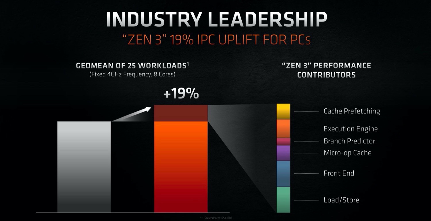
The AMD Ryzen 7 5800U is a processor for thin and light laptops based on the Cezanne generation. The R7 5800U integrates all eight cores based on the Zen 3 microarchitecture and is the fastest U-series processor at launch. They are clocked at 1.9 (guaranteed base clock) to 4.4 GHz (Turbo) and support SMT / Hyperthreading (16 threads). The chip is manufactured on the modern 7 nm TSMC process.
The new Zen 3 microarchitecture offers a significantly higher IPC (instructions per clock) compared to Zen 2. For desktop processors AMD claims 19 percent on average and in applications reviews showed around 12% gains at the same clock speed.
In addition to the eight CPU cores, the APU also integrates a Radeon RX Vega 8 GPU with 8 CUs at up to 2000 MHz. The dual channel memory controller supports DDR4-3200 and energy efficient LPDDR4-4266 RAM. Furthermore, 16 MB level 3 cache (up from 8 MB at the 4800U) can be found on the chip.
Performance
The average 5800U in our database matches the Core i5-11260H and, perhaps a little disappointingly, the Ryzen 7 4800U in multi-core performance.
Thanks to its decent cooling solution and a long-term CPU power limit of 22 W, the ProBook x360 435 G8 is among the fastest laptops powered by the 5800U that we know of. It can be more than 10% faster in CPU-bound workloads than the slowest system featuring the same chip in our database, as of August 2023.
Power consumption
This Ryzen 7 series chip has a default TDP (also known as the long-term power limit) of 15 W, a value that laptop makers are allowed to change to anything between 10 W and 25 W with clock speeds and performance changing accordingly as a result. Choosing the lowest value would allow one to build a passively cooled system around the Ryzen, however, most laptop manufacturers will do the opposite to extract as much performance out of the chip as possible.
The Ryzen 7 5800U is built with TSMC's 7 nm process for average, as of mid 2023, energy efficiency.
Intel Core i7-1250U
► remove from comparisonThe Intel Core i7-1250U is a mobile CPU for thin and light laptops based on the Alder Lake architecture. It was announced in early 2022 and offers 2 performance cores (P-cores, Golden Cove architecture) and 8 efficient cores (E-cores, Gracemont architecture). The P-cores support Hyper-Threading leading to 12 supported threads when combined with the E-cores. The clock rate ranges from 1.1 to 4.7 GHz on the performance cluster and 0.8 to 3.5 GHz on the efficient cluster. The performance of the E-cores should be similar to old Skylake cores (compare to the Core i7-6700HQ). All cores can use up to 12 MB L3 cache. Compared to the similar Core i7-1260U, the 1250U only offers "Essentials" vPro management features.
Performance
The average 1250U in our database is in the same league as the Ryzen 5 5500U; the i5-1240U, the i7-1260U and the i7-1265U are found close nearby as well.
Thanks to its decent cooling solution and a long-term CPU power limit of 23 W, the Envy x360 13-bf0013dx is among the fastest laptops built around the 1250U that we know of. It can be at least 30% faster in CPU-bound workloads than the slowest system featuring the same chip in our database, as of August 2023.
Features
The integrated memory controller supports various memory types up to DDR5-4800, DDR4-3200, LPDDR5-5200, and LPDDR4x-4267. The Thread Director (in hardware) can support the operating system to decide which thread to use on the performance or efficient cores for the best performance. For AI tasks, the CPU also integrates GNA 3.0 and DL Boost (via AVX2). Quick Sync in version 8 is the same as in the Rocket Lake CPUs and supports MPEG-2, AVC, VC-1 decode, JPEG, VP8 decode, VP9, HEVC, and AV1 decode in hardware. The CPU only supports PCIe 4.0 (x8 for a GPU and two x4 for SSDs).
The integrated graphics adapter is based on the Xe architecture and offers all 96 EUs (Execution Units) operating at up to 0.95 GHz.
The CPU is rated at 9 W base power (TDP, PL1) and 29 W max. Turbo power (PL2) and the whole SoC is manufactured on a 10nm process at Intel, which is known as Intel 7.
| Model | Intel Celeron 7300 | AMD Ryzen 7 5800U | Intel Core i7-1250U | ||||||||||||||||||||||||||||||||||||||||||||||||||||||||||||||||||||||||||||||||||||||||||||||||||||||||||||||||||||||||||||||||
| Codename | Alder Lake-U | Cezanne-U (Zen 3) | Alder Lake-U | ||||||||||||||||||||||||||||||||||||||||||||||||||||||||||||||||||||||||||||||||||||||||||||||||||||||||||||||||||||||||||||||||
| Series | Intel Alder Lake-M | AMD Cezanne (Zen 3, Ryzen 5000) | Intel Alder Lake-M | ||||||||||||||||||||||||||||||||||||||||||||||||||||||||||||||||||||||||||||||||||||||||||||||||||||||||||||||||||||||||||||||||
| Series: Alder Lake-M Alder Lake-U |
|
|
| ||||||||||||||||||||||||||||||||||||||||||||||||||||||||||||||||||||||||||||||||||||||||||||||||||||||||||||||||||||||||||||||||
| Clock | 700 - 1000 MHz | 1900 - 4400 MHz | 800 - 4700 MHz | ||||||||||||||||||||||||||||||||||||||||||||||||||||||||||||||||||||||||||||||||||||||||||||||||||||||||||||||||||||||||||||||||
| L1 Cache | 464 KB | 512 KB | 928 KB | ||||||||||||||||||||||||||||||||||||||||||||||||||||||||||||||||||||||||||||||||||||||||||||||||||||||||||||||||||||||||||||||||
| L2 Cache | 3.5 MB | 4 MB | 9.5 MB | ||||||||||||||||||||||||||||||||||||||||||||||||||||||||||||||||||||||||||||||||||||||||||||||||||||||||||||||||||||||||||||||||
| L3 Cache | 8 MB | 16 MB | 12 MB | ||||||||||||||||||||||||||||||||||||||||||||||||||||||||||||||||||||||||||||||||||||||||||||||||||||||||||||||||||||||||||||||||
| Cores / Threads | 5 / 5 1 x 1.0 GHz Intel Golden Cove P-Core 4 x 0.7 GHz Intel Crestmont E-Core | 8 / 16 | 10 / 12 | ||||||||||||||||||||||||||||||||||||||||||||||||||||||||||||||||||||||||||||||||||||||||||||||||||||||||||||||||||||||||||||||||
| TDP | 9 Watt | 25 Watt | 9 Watt | ||||||||||||||||||||||||||||||||||||||||||||||||||||||||||||||||||||||||||||||||||||||||||||||||||||||||||||||||||||||||||||||||
| Technology | 10 nm | 7 nm | 10 nm | ||||||||||||||||||||||||||||||||||||||||||||||||||||||||||||||||||||||||||||||||||||||||||||||||||||||||||||||||||||||||||||||||
| max. Temp. | 100 °C | 105 °C | 100 °C | ||||||||||||||||||||||||||||||||||||||||||||||||||||||||||||||||||||||||||||||||||||||||||||||||||||||||||||||||||||||||||||||||
| Socket | BGA1700 | FP6 | BGA1781 | ||||||||||||||||||||||||||||||||||||||||||||||||||||||||||||||||||||||||||||||||||||||||||||||||||||||||||||||||||||||||||||||||
| Features | Thread Director | DDR4-3200/LPDDR4-4266 RAM, PCIe 3, MMX, SSE, SSE2, SSE3, SSSE3, SSE4A, SSE4.1, SSE4.2, AVX, AVX2, BMI2, ABM, FMA, ADX, SMEP, SMAP, SMT, CPB, AES-NI, RDRAND, RDSEED, SHA, SME | LPDDR4x-4266/LPDDR5-5200 RAM, PCIe 4, Thr. Dir., DL Boost, GNA, vPro Ess., MMX, SSE, SSE2, SSE3, SSSE3, SSE4.1, SSE4.2, AVX, AVX2, BMI2, ABM, FMA, ADX, SMEP, SMAP, EIST, TM1, TM2, HT, Turbo, SST, AES-NI, RDRAND, RDSEED, SHA | ||||||||||||||||||||||||||||||||||||||||||||||||||||||||||||||||||||||||||||||||||||||||||||||||||||||||||||||||||||||||||||||||
| iGPU | Intel UHD Graphics Xe G4 48EUs ( - 800 MHz) | AMD Radeon RX Vega 8 (Ryzen 4000/5000) ( - 2000 MHz) | Intel Iris Xe Graphics G7 96EUs ( - 950 MHz) | ||||||||||||||||||||||||||||||||||||||||||||||||||||||||||||||||||||||||||||||||||||||||||||||||||||||||||||||||||||||||||||||||
| Architecture | x86 | x86 | x86 | ||||||||||||||||||||||||||||||||||||||||||||||||||||||||||||||||||||||||||||||||||||||||||||||||||||||||||||||||||||||||||||||||
| Announced | |||||||||||||||||||||||||||||||||||||||||||||||||||||||||||||||||||||||||||||||||||||||||||||||||||||||||||||||||||||||||||||||||||
| Manufacturer | ark.intel.com | www.amd.com | ark.intel.com |

Benchmarks

Average Benchmarks AMD Ryzen 7 5800U → 0% n=0
Average Benchmarks Intel Core i7-1250U → 0% n=0
* Smaller numbers mean a higher performance
1 This benchmark is not used for the average calculation