

AMD Ryzen 7 H 260 vs AMD Ryzen 7 5700U vs AMD Ryzen 9 PRO 8945HS
AMD Ryzen 7 H 260
► remove from comparison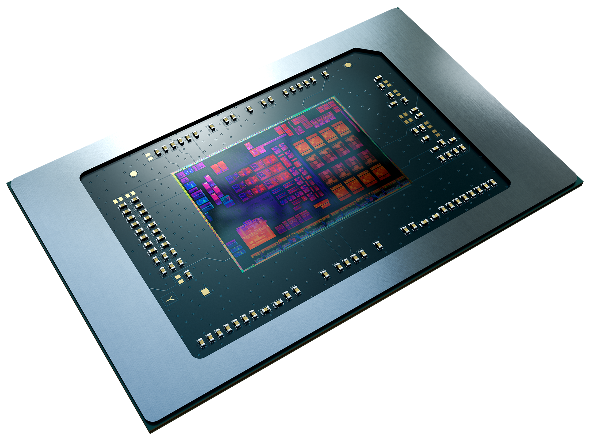
The AMD Ryzen 7 H 260 is a high-end notebook processor from the Hawk Point series with 8 cores and hyperthreading (SMT), which means it can process up to 16 threads simultaneously. At release, the CPU is only available in China and is technically practically identical to the older AMD Ryzen 7 8845HS or Ryzen 7 7840HS (slower AI engine).
The performance of the second-fastest model in the Hawk Point series should only be slightly behind the Ryzen 9 7940HS (+100 - 200 MHz clock, e.g. only 2% slower Turbo). As a result, the performance at 54W TDP should also be comparable to the AMD Ryzen 7 7745HX (also 8 Zen 4 cores, max 5.1 GHz, 55W, 32 MB L3) and thus clearly ahead of the old top model AMD Ryzen 9 6980HX resp. 6980HS (with lower TDP).
The chip integrates a modern RDNA 3-based graphics card (iGPU) called Radeon 780M with 12 CUs and up to 2.7GHz including AV1 video engine. Furthermore, a Xilinx FPGA-based XDNA AI accelerator is also integrated, which is now clocked higher. Hawk Point offers 2x USB 4 (40 Gbps), 20 PCIe 4.0 lanes and a dual-channel DDR5-5600 / LPDDR5x-7500 memory controller (with ECC support).
The Hawk Point series is a single chip (unlike the Dragon Range 7045HX series) and is manufactured at TSMC using the modern 4nm FinFET process.
AMD Ryzen 7 5700U
► remove from comparison
The AMD Ryzen 7 5700U is an APU of the Lucienne product family designed for leaner laptops. The Ryzen features eight Zen 2 cores clocked at 1.8 GHz (base clock speed) to 4.3 GHz (Boost) as well as a Vega 8 iGPU. Thread-doubling SMT tech is enabled in this CPU for up to 16 concurrent processing threads.
Architecture
In spite of what its name may suggest, Ryzen 7 5700U is not a Zen 3 part, meaning this is a Ryzen 4000 series mobile processor in disguise. Nevertheless, the CPU is manufactured on the modern 7 nm TSMC process and its performance as well as energy efficiency figures are very strong compared to what Intel currently has to offer in this segment.
The Ryzen 7 features 8 MB of Level 3 cache. Its built-in memory controller is designed to work with dual-channel DDR4-3200 or quad-channel LPDDR4-4266 RAM. Unlike the desktop Ryzen 5000 processors, Ryzen 7 5700U does not support PCI-Express 4.0, meaning those speedy NVMe SSDs will be limited to read/write rates of 3.9 GB/s.
The Ryzen gets soldered directly to the motherboard (FP6 socket) and is thus not user-replaceable.
Performance
The average 5700U in our database is in the same league as the Ryzen 7 4800U, Ryzen 7 PRO 5850U, Core i7-1365U, as far as multi-thread benchmark scores are concerned.
Thanks to its decent cooling solution and a long-term CPU power limit of 35 W, the Schenker VIA 15 Pro is among the fastest laptops built around the 5700U that we know of. It can be roughly 50% faster in CPU-bound workloads than the slowest system featuring the same chip in our database, as of August 2023.
Graphics
In addition to its eight CPU cores, Ryzen 7 5700U features a Radeon RX Vega series graphics adapter with 8 CUs (= 512 shaders) running at up to 1,900 MHz. This iGPU trails behind the 96 EU Intel Iris Xe Graphics G7 in synthetic benchmarks, yet its real-world performance is good enough for many games released in 2020 and 2021 at reasonable resolutions (up to Full HD 1080p) and low to medium quality. As the Vega has no VRAM of its own, it is paramount that fast system RAM is used.
The graphics adapter definitely supports UHD 2160p monitors at 60 Hz, and will gladly HW-decode AVC, HEVC and VP9-encoded videos. There is no AV1 support here though.
Power consumption
This Ryzen 7 has a default TDP, also known as the long-term power limit, of 15 W; laptop makers are free to change that to anything between 10 W and 25 W, with clock speeds and performance changing accordingly as a result. Most companies will go for a higher value to extract more performance out of the APU. By choosing the lowest value, it will be possible to build a passively cooled system around the chip, too.
The 7 nm TSMC process the R7 5700U is built with makes for decent, as of late 2022, energy efficiency.
AMD Ryzen 9 PRO 8945HS
► remove from comparisonThe Ryzen 9 PRO 8945HS is a powerful Hawk Point family processor (APU) released in April 2024. The R9 PRO 8945HS is identical to the "normal" R9 8945HS in virtually all respects; both come with 8 Zen 4 cores running at 4.0 GHz to 5.2 GHz (16 processing threads), a 16-TOPS Ryzen AI NPU (higher clock speeds) and the top-of-the-line Radeon 780M graphics adapter. Other key features include PCIe 4 and USB 4 support, LPDDR5x-7500 RAM support and 16 MB of L3 cache. Unlike the R9 8945HS however this PRO series chip has ECC memory support and the Secure Processor feature which in a nutshell is an ARM co-processor built into the main chip.
Architecture and Features
Hawk Point APUs are powered by the Zen 4 architecture, just like Dragon Range, Phoenix and Raphael processors are. With this product family, AMD is betting big on generative AI; these chips are said to deliver an up to 40% increase in generative AI performance over 7040 series APUs making apps like DaVinci Resolve and Adobe Photoshop more powerful than ever before.
Unlike Zen 3, Zen 4 features AVX512 support and, thanks to a plethora of other improvements including larger registers/buffers/caches (reportedly at the cost of some of them becoming slightly slower), is supposed to bring an IPC improvement of around 13%.
Elsewhere, the R9 PRO 8945HS has 16 MB of L3 cache and support for super-fast RAM (up to LPDDR5x-7500 or DDR5-5600 with ECC support optionally present depending on the socket). The processor is compatible with USB 4 and thus with Thunderbolt; PCIe support is limited to the 4.0 spec for a throughput of 1.97 GB/s per lane. 20 lanes are available.
OS support is limited to 64-bit editions of Windows 11 and Windows 10 and of course to Linux. Note that the chip isn't overclockable and neither is it user-replaceable as it gets soldered down for good (FP7, FP7r2, FP8 socket interfaces).
Performance
The 8945HS is an R9 7940HS in disguise, so it's realistic to expect the chip to be just slightly faster than the Core i9-12900HK and also the Ryzen 7 7840HS, as far as multi-thread performance is concerned.
Your mileage may vary depending on how high the CPU power limits are and how competent the cooling solution of your system is.
Graphics
The Radeon 780M has 12 CUs (768 shaders) running at up to 2,800 MHz. This is a very fast iGPU, as of late 2023. It will let you use up to 4 monitors with resolutions as high as SUHD 4320p, and it is also capable of HW-encoding and HW-decoding the most widely used video codecs including AVC, HEVC and AV1. More importantly, it is fast enough for proper 1080p gaming as long as one is fine with low to medium detail settings.
Your mileage may vary depending on how high the CPU power limits are, how competent the cooling solution of the system is, how fast the RAM of the system is (there is no dedicated VRAM here).
Power consumption
This Ryzen 9 series chip has a long-term power limit (default TDP) of 35 W to 54 W, giving laptop makers a choice between longer battery life and higher performance. Either way, an active cooling solution is a must for a system powered by this chip.
The 8945HS is built with TSMC's 4 nm process for high, as of late 2023, energy efficiency.
| Model | AMD Ryzen 7 H 260 | AMD Ryzen 7 5700U | AMD Ryzen 9 PRO 8945HS | ||||||||||||||||||||||||||||||||||||||||||||||||||||||||||||||||||||||||||||||||||||||||||||||||||||||||||||||||||||||||||||
| Codename | Hawk Point-HS (Zen 4) | Lucienne-U (Zen 2) | Hawk Point-HS (Zen 4) | ||||||||||||||||||||||||||||||||||||||||||||||||||||||||||||||||||||||||||||||||||||||||||||||||||||||||||||||||||||||||||||
| Series | AMD Hawk Point (Zen 4/4c) | AMD Lucienne (Zen 2, Ryzen 5000) | AMD Hawk Point (Zen 4/4c) | ||||||||||||||||||||||||||||||||||||||||||||||||||||||||||||||||||||||||||||||||||||||||||||||||||||||||||||||||||||||||||||
| Series: Hawk Point (Zen 4/4c) Hawk Point-HS (Zen 4) |
|
|
| ||||||||||||||||||||||||||||||||||||||||||||||||||||||||||||||||||||||||||||||||||||||||||||||||||||||||||||||||||||||||||||
| Clock | 3800 - 5100 MHz | 1800 - 4300 MHz | 4000 - 5200 MHz | ||||||||||||||||||||||||||||||||||||||||||||||||||||||||||||||||||||||||||||||||||||||||||||||||||||||||||||||||||||||||||||
| L1 Cache | 512 KB | 512 KB | 512 KB | ||||||||||||||||||||||||||||||||||||||||||||||||||||||||||||||||||||||||||||||||||||||||||||||||||||||||||||||||||||||||||||
| L2 Cache | 8 MB | 4 MB | 8 MB | ||||||||||||||||||||||||||||||||||||||||||||||||||||||||||||||||||||||||||||||||||||||||||||||||||||||||||||||||||||||||||||
| L3 Cache | 16 MB | 8 MB | 16 MB | ||||||||||||||||||||||||||||||||||||||||||||||||||||||||||||||||||||||||||||||||||||||||||||||||||||||||||||||||||||||||||||
| Cores / Threads | 8 / 16 8 x 5.1 GHz AMD Zen 4 | 8 / 16 | 8 / 16 8 x 5.2 GHz AMD Zen 4 | ||||||||||||||||||||||||||||||||||||||||||||||||||||||||||||||||||||||||||||||||||||||||||||||||||||||||||||||||||||||||||||
| TDP | 45 Watt | 25 Watt | 45 Watt | ||||||||||||||||||||||||||||||||||||||||||||||||||||||||||||||||||||||||||||||||||||||||||||||||||||||||||||||||||||||||||||
| Technology | 4 nm | 7 nm | 4 nm | ||||||||||||||||||||||||||||||||||||||||||||||||||||||||||||||||||||||||||||||||||||||||||||||||||||||||||||||||||||||||||||
| Die Size | 178 mm2 | 178 mm2 | |||||||||||||||||||||||||||||||||||||||||||||||||||||||||||||||||||||||||||||||||||||||||||||||||||||||||||||||||||||||||||||
| max. Temp. | 100 °C | 105 °C | 100 °C | ||||||||||||||||||||||||||||||||||||||||||||||||||||||||||||||||||||||||||||||||||||||||||||||||||||||||||||||||||||||||||||
| Socket | FP7/FP7r2/FP8 | FP6 | FP7/FP7r2 | ||||||||||||||||||||||||||||||||||||||||||||||||||||||||||||||||||||||||||||||||||||||||||||||||||||||||||||||||||||||||||||
| Features | DDR5-5600/LPDDR5x-7500 RAM, PCIe 4, Ryzen AI, MMX, SSE, SSE2, SSE3, SSSE3, SSE4A, SSE4.1, SSE4.2, AVX, AVX2, AVX-512, BMI2, ABM, FMA, ADX, SMEP, SMAP, SMT, CPB, AES-NI, RDRAND, RDSEED, SHA, SME | DDR4-3200/LPDDR4-4266 RAM, PCIe 3, MMX, SSE, SSE2, SSE3, SSSE3, SSE4A, SSE4.1, SSE4.2, AVX, AVX2, BMI2, ABM, FMA, ADX, SMEP, SMAP, SMT, CPB, AES-NI, RDRAND, RDSEED, SHA, SME | DDR5-5600/LPDDR5x-7500 RAM, PCIe 4, Ryzen AI, MMX, SSE, SSE2, SSE3, SSSE3, SSE4A, SSE4.1, SSE4.2, AVX, AVX2, AVX-512, BMI2, ABM, FMA, ADX, SMEP, SMAP, SMT, CPB, AES-NI, RDRAND, RDSEED, SHA, SME | ||||||||||||||||||||||||||||||||||||||||||||||||||||||||||||||||||||||||||||||||||||||||||||||||||||||||||||||||||||||||||||
| iGPU | AMD Radeon 780M ( - 2700 MHz) | AMD Radeon RX Vega 8 (Ryzen 4000/5000) ( - 1900 MHz) | AMD Radeon 780M ( - 2800 MHz) | ||||||||||||||||||||||||||||||||||||||||||||||||||||||||||||||||||||||||||||||||||||||||||||||||||||||||||||||||||||||||||||
| Architecture | x86 | x86 | x86 | ||||||||||||||||||||||||||||||||||||||||||||||||||||||||||||||||||||||||||||||||||||||||||||||||||||||||||||||||||||||||||||
| Announced | |||||||||||||||||||||||||||||||||||||||||||||||||||||||||||||||||||||||||||||||||||||||||||||||||||||||||||||||||||||||||||||||
| Manufacturer | www.amd.com | www.amd.com | www.amd.com |

Benchmarks

Average Benchmarks AMD Ryzen 7 5700U → 0% n=0
* Smaller numbers mean a higher performance
1 This benchmark is not used for the average calculation