

Intel Processor U300 vs AMD Ryzen 5 PRO 7640U vs AMD Ryzen 5 PRO 7640HS
Intel Processor U300
► remove from comparison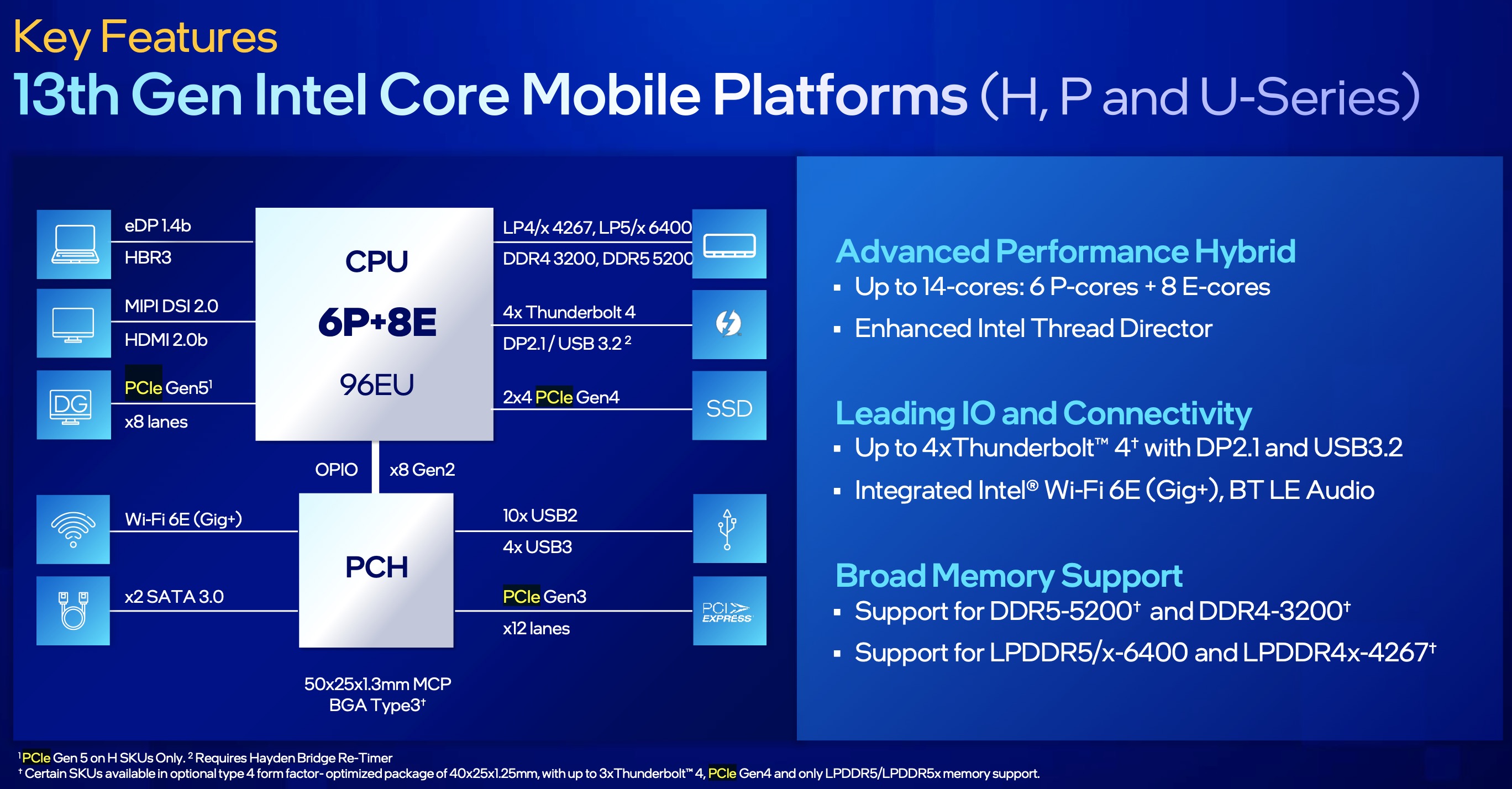
The Intel Processor U300 is an entry-level mobile CPU for thin and light laptops of the Raptor Lake-U series. It was announced in early 2023 and offers one performance core (Raptor Cove architecture P-core, similar to Alder Lake) and 4 efficient cores (E-cores, Gracemont architecture). The P-cores support Hyper-Threading for 6 processing threads when combined with the E-cores. The clock rate ranges from 1.2 to 4.4 GHz on the performance cluster and 0.9 to 3.3 GHz on the efficient cluster. The per-clock performance of the E-cores should be similar to old Skylake cores (compare to the Core i7-6700HQ). All cores have access to 8 MB of L3 cache.
Performance
While we have not tested a single system powered by the U300 as of February 2024, its performance should be very similar to the outgoing Alder Lake Pentium 8505, since there is little difference between the two. The average U300 is set to be 10% to 20% behind the Ryzen 3 5300U and the Core i7-1185G7, as far as multi-thread benchmark scores are concerned, making the former an entry-level chip as of early 2024.
Your mileage may vary depending on how high the CPU power limits are.
Features
The integrated memory controller supports various memory types up to DDR5-4800, DDR4-3200, LPDDR5-5200, and LPDDR4x-4267. The Thread Director (in hardware) can support the operating system to decide which thread to use on the performance or efficient cores for the best performance. For AI tasks, the CPU also integrates GNA 3.0 and DL Boost (via AVX2). Quick Sync in version 8 is the same as in the Rocket Lake CPUs and supports MPEG-2, AVC, VC-1 decode, JPEG, VP8 decode, VP9, HEVC, and AV1 decode in hardware. Several PCIe 4 lanes (x8 for a GPU and two x4 for SSDs) as well as several PCIe 3 lanes are on offer.
The integrated graphics adapter is based on the Xe architecture and offers 48 of the 96 EUs (Execution Units) operating at up to 1.1 GHz.
Power consumption
The U300 has a base power consumption of 15 W, with 55 W being its maximum Intel-recommended Turbo power consumption. The CPU is built with a 10 nm process marketed as Intel 7.
AMD Ryzen 5 PRO 7640U
► remove from comparison
The AMD Ryzen 5 PRO 7640U is a fast mid-range laptop processor of the Phoenix series. It offers 6 cores (hexa core) based on the Zen 4 architecture that supports hyperthreading (12 threads). The cores clock from 3.5 (base) up to 4.9 GHz (single core boost). The processor includes 6 MB L2 cache and 16 MB L3 cache.
Compared to the consumer Ryzen 5 7640U, the PRO models offer additional security, manageability, and reliability features designed for professional users and workstation environments.
Thanks to the new Zen 4 architecture and higher clock speeds, the R5 PRO 7640U is clearly faster than the old Ryzen 5 6600U (Zen 3, 6 cores, 4.5 GHz). Compared to the similar 7640HS, the U-series offers a lower TDP and slightly lower core clocks.
The chip integrates a modern and fasts RDNA 3 graphics card (iGPU) called Radeon 760M with 8 of the 12 CUs and 2.6 GHz clock speed. Furthermore, the Phoenix series include a video engine with AV1 de- and encoding, a new Xilinx FPGA based XDNA AI accelerator (Ryzen AI) that should be faster than the AI engine in the Apple M2 SOC and a dual-channel DDR5-5600 / LPDDR5x-7500 memory controller (with ECC support). The connectivity features includes 2 possible USB 4 (40 Gbps) ports and 20 PCIe 4.0 lanes for a GPU and SSDs.
The Phoenix series uses a single monolithic design (unlike the chiplet design of the 7045HX series) and is manufactured in the modern 4nm process at TSMC. The TDP can be configured between 35 and 45 Watt.
AMD Ryzen 5 PRO 7640HS
► remove from comparisonThe AMD Ryzen 5 PRO 7640HS is a fast mid-range laptop processor of the Phoenix series. It offers 6 cores (hexa core) based on the Zen 4 architecture that supports hyperthreading (12 threads). The cores clock from 4.3 (base) up to 5 GHz (single core boost). The processor includes 6 MB L2 cache and 16 MB L3 cache.
Compared to the consumer Ryzen 5 7640HS, the PRO models offer additional security, manageability, and reliability features designed for professional users and workstation environments.
The performance of the R5 PRO 7640HS is clearly lower (multi-threaded) than the higher end Ryzen 7 7840HS and Ryzen 9 7940HS models due to the two missing CPU cores. Compared to the faster HX series, the 7640HS at 54W TDP should be only slightly slower than the Ryzen 5 7645HX (also 6 Zen 4 cores, up to 5 GHz, 55W). The old Ryzen 5 6600H should be easily bested thanks to the improved architecture and higher clock speeds.
The chip integrates a modern and fasts RDNA 3 graphics card (iGPU) called Radeon 760M with 8 of the 12 CUs and 2.6 GHz clock speed. Furthermore, the Phoenix series include a video engine with AV1 de- and encoding, a new Xilinx FPGA based XDNA AI accelerator (Ryzen AI) that should be faster than the AI engine in the Apple M2 SOC and a dual-channel DDR5-5600 / LPDDR5x-7500 memory controller (with ECC support). The connectivity features includes 2 possible USB 4 (40 Gbps) ports and 20 PCIe 4.0 lanes for a GPU and SSDs.
The Phoenix series uses a single monolithic design (unlike the chiplet design of the 7045HX series) and is manufactured in the modern 4nm process at TSMC. The TDP can be configured between 35 and 45 Watt.
| Model | Intel Processor U300 | AMD Ryzen 5 PRO 7640U | AMD Ryzen 5 PRO 7640HS | ||||||||||||||||||||||||||||||||||||||||||||||||||||||||||||||||||||||||||||||||||||||||
| Codename | Raptor Lake-U | Phoenix (Zen4) | Phoenix (Zen4) | ||||||||||||||||||||||||||||||||||||||||||||||||||||||||||||||||||||||||||||||||||||||||
| Series | Intel Raptor Lake-U | AMD Phoenix (Zen 4) | AMD Phoenix (Zen 4) | ||||||||||||||||||||||||||||||||||||||||||||||||||||||||||||||||||||||||||||||||||||||||
| Series: Phoenix (Zen 4) Phoenix (Zen4) |
|
|
| ||||||||||||||||||||||||||||||||||||||||||||||||||||||||||||||||||||||||||||||||||||||||
| Clock | 900 - 4400 MHz | 3500 - 4900 MHz | 4300 - 5000 MHz | ||||||||||||||||||||||||||||||||||||||||||||||||||||||||||||||||||||||||||||||||||||||||
| L1 Cache | 464 KB | 384 KB | 384 KB | ||||||||||||||||||||||||||||||||||||||||||||||||||||||||||||||||||||||||||||||||||||||||
| L2 Cache | 3.5 MB | 6 MB | 6 MB | ||||||||||||||||||||||||||||||||||||||||||||||||||||||||||||||||||||||||||||||||||||||||
| L3 Cache | 8 MB | 16 MB | 16 MB | ||||||||||||||||||||||||||||||||||||||||||||||||||||||||||||||||||||||||||||||||||||||||
| Cores / Threads | 5 / 6 1 x 4.4 GHz Intel Raptor Cove P-Core 4 x 3.3 GHz Intel Gracemont E-Core | 6 / 12 6 x 4.9 GHz AMD Zen 4 | 6 / 12 | ||||||||||||||||||||||||||||||||||||||||||||||||||||||||||||||||||||||||||||||||||||||||
| TDP | 15 Watt | 15 Watt | 54 Watt | ||||||||||||||||||||||||||||||||||||||||||||||||||||||||||||||||||||||||||||||||||||||||
| TDP Turbo PL2 | 55 Watt | ||||||||||||||||||||||||||||||||||||||||||||||||||||||||||||||||||||||||||||||||||||||||||
| Technology | 10 nm | 4 nm | 4 nm | ||||||||||||||||||||||||||||||||||||||||||||||||||||||||||||||||||||||||||||||||||||||||
| max. Temp. | 100 °C | 100 °C | 100 °C | ||||||||||||||||||||||||||||||||||||||||||||||||||||||||||||||||||||||||||||||||||||||||
| Socket | BGA1744 | ||||||||||||||||||||||||||||||||||||||||||||||||||||||||||||||||||||||||||||||||||||||||||
| Features | DDR4-3200/LPDDR4x-4267/DDR5-5200/LPDDR5-5200/LPDDR5x-5200 RAM, PCIe 4, Thr. Director, DL Boost, GNA, MMX, SSE, SSE2, SSE3, SSSE3, SSE4.1, SSE4.2, AVX, AVX2, BMI2, ABM, FMA, ADX, VMX, SMEP, SMAP, EIST, TM1, TM2, HT, Turbo, SST, AES-NI, RDRAND, RDSEED, SHA | ||||||||||||||||||||||||||||||||||||||||||||||||||||||||||||||||||||||||||||||||||||||||||
| iGPU | Intel UHD Graphics Xe G4 48EUs ( - 1100 MHz) | AMD Radeon 760M ( - 2600 MHz) | AMD Radeon 760M ( - 2600 MHz) | ||||||||||||||||||||||||||||||||||||||||||||||||||||||||||||||||||||||||||||||||||||||||
| Architecture | x86 | x86 | x86 | ||||||||||||||||||||||||||||||||||||||||||||||||||||||||||||||||||||||||||||||||||||||||
| Announced | |||||||||||||||||||||||||||||||||||||||||||||||||||||||||||||||||||||||||||||||||||||||||||
| Manufacturer | ark.intel.com | www.amd.com | www.amd.com | ||||||||||||||||||||||||||||||||||||||||||||||||||||||||||||||||||||||||||||||||||||||||
| Die Size | 178 mm2 | 178 mm2 | |||||||||||||||||||||||||||||||||||||||||||||||||||||||||||||||||||||||||||||||||||||||||
| NPU / AI | 10 TOPS INT8 | ||||||||||||||||||||||||||||||||||||||||||||||||||||||||||||||||||||||||||||||||||||||||||
| Chip AI | 25 TOPS INT8 |

Benchmarks
Average Benchmarks Intel Processor U300 → 0% n=0
Average Benchmarks AMD Ryzen 5 PRO 7640HS → 0% n=0
* Smaller numbers mean a higher performance
1 This benchmark is not used for the average calculation