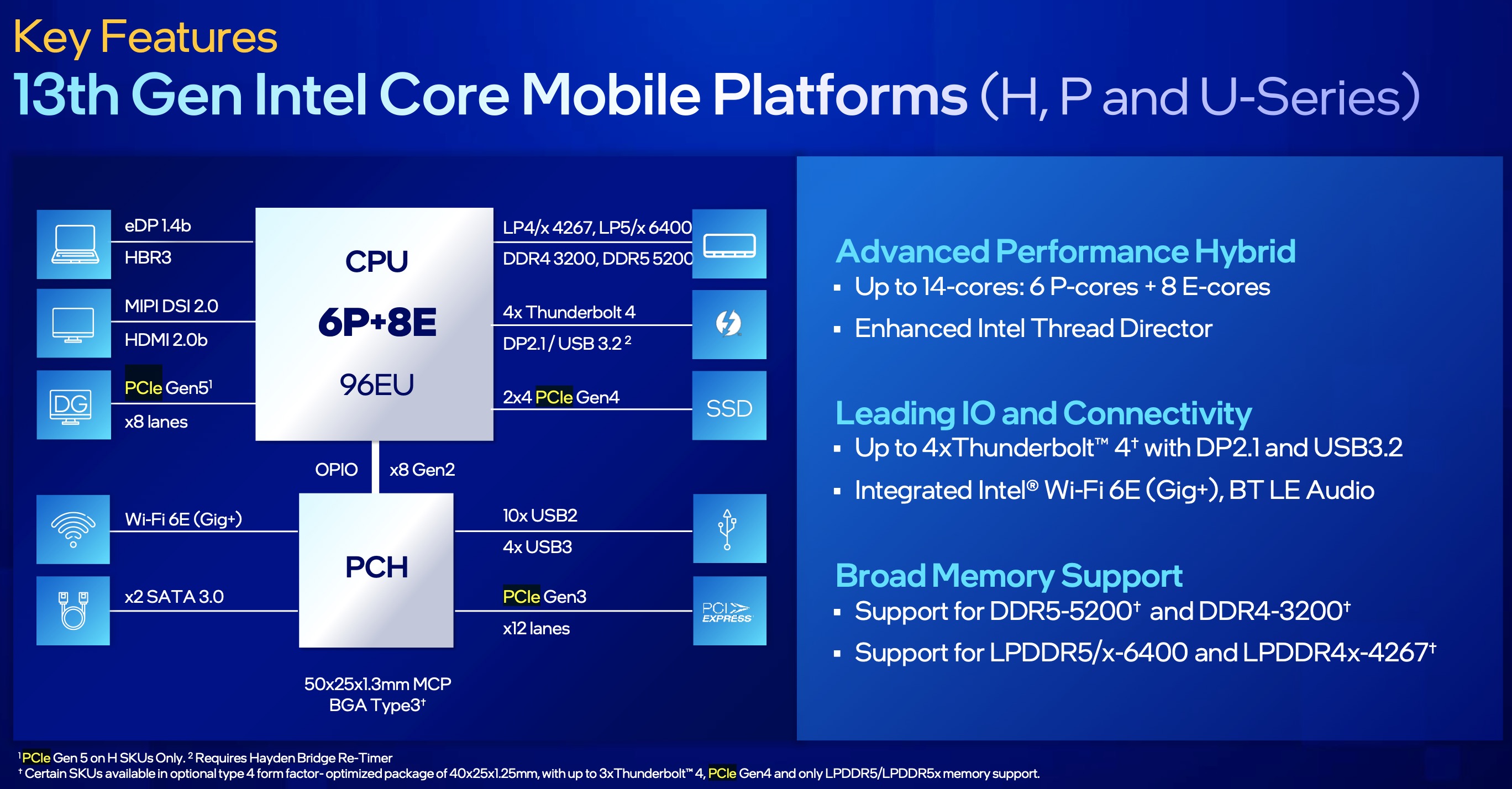
The Intel Processor U300 is an entry-level mobile CPU for thin and light laptops of the Raptor Lake-U series. It was announced in early 2023 and offers one performance core (Raptor Cove architecture P-core, similar to Alder Lake) and 4 efficient cores (E-cores, Gracemont architecture). The P-cores support Hyper-Threading for 6 processing threads when combined with the E-cores. The clock rate ranges from 1.2 to 4.4 GHz on the performance cluster and 0.9 to 3.3 GHz on the efficient cluster. The per-clock performance of the E-cores should be similar to old Skylake cores (compare to the Core i7-6700HQ). All cores have access to 8 MB of L3 cache.
Performance
While we have not tested a single system powered by the U300 as of February 2024, its performance should be very similar to the outgoing Alder Lake Pentium 8505, since there is little difference between the two. The average U300 is set to be 10% to 20% behind the Ryzen 3 5300U and the Core i7-1185G7, as far as multi-thread benchmark scores are concerned, making the former an entry-level chip as of early 2024.
Your mileage may vary depending on how high the CPU power limits are.
Features
The integrated memory controller supports various memory types up to DDR5-4800, DDR4-3200, LPDDR5-5200, and LPDDR4x-4267. The Thread Director (in hardware) can support the operating system to decide which thread to use on the performance or efficient cores for the best performance. For AI tasks, the CPU also integrates GNA 3.0 and DL Boost (via AVX2). Quick Sync in version 8 is the same as in the Rocket Lake CPUs and supports MPEG-2, AVC, VC-1 decode, JPEG, VP8 decode, VP9, HEVC, and AV1 decode in hardware. Several PCIe 4 lanes (x8 for a GPU and two x4 for SSDs) as well as several PCIe 3 lanes are on offer.
The integrated graphics adapter is based on the Xe architecture and offers 48 of the 96 EUs (Execution Units) operating at up to 1.1 GHz.
Power consumption
The U300 has a base power consumption of 15 W, with 55 W being its maximum Intel-recommended Turbo power consumption. The CPU is built with a 10 nm process marketed as Intel 7.
The AMD Ryzen 5 7535HS is a processor for big (gaming) laptops based of the Rembrandt Refresh generation. The R5 7535HS integrates six of the eight cores based on the Zen 3+ microarchitecture. They are clocked at 3.3 (guaranteed base clock) to 4.55 GHz (boost) and support SMT / Hyperthreading (12 threads). The 7535HS is a refresh of the old Ryzen 5 6600HS / 6600H with 50 MHz higher boost clock speed.
The Zen 3+ architecture is a refresh of Zen 3 and should not offer a lot of changes. The chip itself however, offers some modern features, like support for USB 4 (40 Gbps), PCI-E Gen 4 and DDR5-4800MT/s or LPDDR5-6400MT/s.
In the 6000 series, AMD switched to the RDNA 2 graphics architecture for the iGPU. As the 6600HS the 7535HS only offers the slower Radeon 660M with 6 of the 12 CUs enabled and 1.9 GHz max. clock rate.
The TDP of the APU is specified from 35 to 54 Watt. The monolithic chip is manufactured in 6nm at TSMC.
Average Benchmarks Intel Processor U300 → 100%n=37
Average Benchmarks AMD Ryzen 5 7535HS → 160%n=37
- Range of benchmark values for this graphics card - Average benchmark values for this graphics card * Smaller numbers mean a higher performance 1 This benchmark is not used for the average calculation
v1.33
log 27. 21:36:15
#0 ran 0s before starting gpusingle class +0s ... 0s
#1 checking url part for id 14924 +0s ... 0s
#2 checking url part for id 14954 +0s ... 0s
#3 redirected to Ajax server, took 1759001775s time from redirect:0 +0s ... 0s
#4 did not recreate cache, as it is less than 5 days old! Created at Thu, 25 Sep 2025 05:17:37 +0200 +0s ... 0s
#5 composed specs +0.005s ... 0.005s
#6 did output specs +0s ... 0.005s
#7 getting avg benchmarks for device 14924 +0.004s ... 0.009s
#8 got single benchmarks 14924 +0.005s ... 0.014s
#9 getting avg benchmarks for device 14954 +0.004s ... 0.018s
#10 got single benchmarks 14954 +0.009s ... 0.028s
#11 got avg benchmarks for devices +0s ... 0.028s
#12 min, max, avg, median took s +0.042s ... 0.069s