The Intel Celeron J4125 is a quad-core SoC primarily for inexpensive mini PCs and was announced late 2019. It runs at 2-2.7 GHz (Single Core Burst) and is based on the Gemini Lake platform (2019 refresh). Compared to the predecessor, the refresh offers slightly higher clock speeds. Similar to the Apollo Lake predecessors, the chip is manufactured on a 14 nm process with FinFETs but offers slightly improved processor cores, double the amount of L2 cache, partial Wi-Fi 5 support, all in a smaller package. Besides four CPU cores, the chip also includes a DirectX 12 capable GPU as well as a DDR4/LPDDR4 memory controller (dual-channel, up to 2400 MHz). The processor is not replaceable as it is directly soldered to the mainboard.
Architecture
The processor architecture is still called Goldmont Plus. Compared to the older Goldmont cores in Apollo Lake, they feature an increased level 2 cache (to 4 MB). That means the per-clock-performance should be a bit better, but not near the Core CPUs like Kaby Lake Y.
Performance
The average J4125 in our database outguns the AMD 3050e just slightly, the latter being a dual-core, Zen-based, entry-level processor of nearly the same energy efficiency, as far as multi-thread benchmark scores are concerned. This means the Celeron is a very basic CPU that's good for basic day-to-day activities only.
The Beelink GK Mini is one of the fastest systems built around the J4125 that we know of. It can be roughly 70% faster in CPU-bound workloads than the slowest system featuring the same chip in our database, as of August 2023.
GPU Performance
The UHD Graphics 600 (Gemini Lake) is based on Intel's Gen9 architecture, which supports DirectX 12 and is also used for the Kaby Lake / Skylake / Apollo Lake graphics adapters (like HD Graphics 520). Equipped with 12 EUs and a clock of up to 750 MHz, the performance should be roughly on par with the older HD Graphics 500 (Apollo Lake).
The chip also includes an advanced video engine with hardware support for the playback of VP9 and H.265 material (8-bit color-depth).
Power consumption
Like most J-class Intel processors, the Celeron has a default TDP, also known as the long-term power limit, of 10 W. This is low enough, allowing laptop makers to ditch fans while building a passively cooled laptop, tablet or mini-PC around the chip.
The Intel Celeron J4125 is built with one of the old 14 nm Intel processes for poor, as of early 2023, energy efficiency.
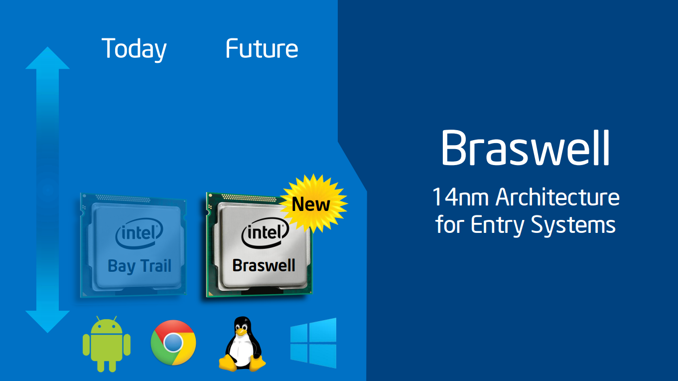
The Intel Celeron N3050 is a low-end dual-core SoC for notebooks, which has been presented in April 2015. It is clocked at 1.6 - 2.16 GHz and part of the Braswell platform. Thanks to its new 14 nanometer low-power process (P1273) with tri-gate transistors, energy efficiency has been significantly improved compared to its predecessor Bay Trail (e.g. Celeron N2840). In addition to the CPU cores, the SoC offers a DirectX 11.2-capable GPU as well as a DDR3L Memory Controller (2x 64 bit, 25.6 GB/s).
Architecture
The processor cores are based on the Airmont architecture, which is basically a slightly modified shrink of the previous Silvermont core. While performance per clock has not been improved, the more efficient 14 nm process leads to a better utilization of the CPU Burst (alias Turbo Boost) and a therefore somewhat higher overall performance.
Performance
Compared to its predecessor Celeron N2815 (1.86 - 2.13 GHz), the N3050 offers an almost identical performance. Using Windows, the CPU is adequate for simple everyday tasks such as light Internet browsing or office applications, but not for complex software or modern games.
Graphics
The HD Graphics (Braswell) is based on the Intel Gen8 architecture, which supports DirectX 11.2 and is also found in the Broadwell series (e.g. HD Graphics 5300). With 12 EUs (Execution Units) and a clock speed of up to 600 MHz, the GPU is almost twice as fast as the HD Graphics (Bay Trail), but still not powerful enough to handle modern 3D games. The GPU also supports 4K/H.265 video acceleration.
Power Consumption
The entire SoC is rated at an TDP of 6 watts (SDP 4 watts). Thus, the chip can be cooled passively.
The Intel Celeron N3160 is a quad-core SoC for entry-level notebooks, which has been announced in early 2016. It is clocked at 1.6 - 2.24 GHz (Burst) and part of the Braswell platform. It is manufactured in a modern 14-nm process (P1273) with FinFETs. In addition to the four CPU cores, the SoC offers a DirectX 11.2-capable GPU as well as a DDR3L Memory Controller (2x 64 bit, 25.6 GB/s). Compared to the predecessor Celeron N3150, the N3160 has a 160 MHz higher Burst clock.
Architecture
The processor cores are based on the Airmont architecture, which is basically a slightly modified shrink of the previous Silvermont core. While performance per clock has not been improved, the more efficient 14 nm process may lead to a better utilization of the CPU Burst (alias Turbo Boost) and therefore a somewhat higher performance in certain situations. The per-MHz performance is still much lower compared to the more expensive Core series (e. g. Broadwell).
Performance
With 4 CPU cores and a clock between 1.6-2.24 GHz, the technical specifications are similar to the previous Celeron N2930, so the processor performance is only slightly better. This means the processor is well-suited for everyday tasks (office, browsing) and even light multi-tasking should be no problem.
Graphics
The HD Graphics (Braswell) is based on the Intel Gen8 architecture, which supports DirectX 11.2 and is also found in the Broadwell series (e.g. HD Graphics 5300). With 12 EUs (Execution Units) and a clock speed of up to 640 MHz, however, the GPU performance is much lower. On average, the GPU is almost twice as fast as the HD Graphics (Bay Trail), so its a bit slower than the older HD Graphics 4000. Only older and simpler titles like Counter Strike: GO will run smoothly. The chip still includes an advanced video unit with support for 4K/H.265 video acceleration.
Power Consumption
The entire SoC is rated at an TDP of 6 watts (SDP 4 watts). Thus, the chip can usually be cooled passively.
- Range of benchmark values for this graphics card - Average benchmark values for this graphics card * Smaller numbers mean a higher performance 1 This benchmark is not used for the average calculation
v1.33
log 19. 15:16:33
#0 ran 0s before starting gpusingle class +0s ... 0s
#1 checking url part for id 12749 +0s ... 0s
#2 checking url part for id 6781 +0s ... 0s
#3 checking url part for id 8167 +0s ... 0s
#4 redirected to Ajax server, took 1755609393s time from redirect:0 +0s ... 0s
#5 did not recreate cache, as it is less than 5 days old! Created at Tue, 19 Aug 2025 05:19:27 +0200 +0s ... 0s
#6 composed specs +0.009s ... 0.009s
#7 did output specs +0s ... 0.009s
#8 getting avg benchmarks for device 12749 +0.004s ... 0.013s
#9 got single benchmarks 12749 +0.008s ... 0.02s
#10 getting avg benchmarks for device 6781 +0.001s ... 0.021s
#11 got single benchmarks 6781 +0.015s ... 0.036s
#12 getting avg benchmarks for device 8167 +0.001s ... 0.037s
#13 got single benchmarks 8167 +0.005s ... 0.042s
#14 got avg benchmarks for devices +0s ... 0.042s
#15 min, max, avg, median took s +0.044s ... 0.086s