

AMD Ryzen 3 5300U vs Intel Pentium 8505 vs Intel Core i5-1230U
AMD Ryzen 3 5300U
► remove from comparison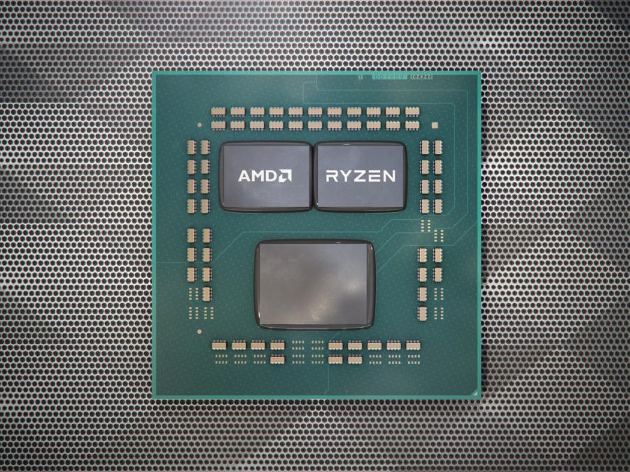
The AMD Ryzen 3 5300U (not to be confused with the A4-5300, a CPU released in 2012) is a Lucienne family processor designed for use in thin and light laptops. The R3 5300U integrates four cores (quad core) based on the Zen 2 microarchitecture. They are clocked at 2.6 (guaranteed base clock) to 3.8 GHz (Turbo) and support SMT for a total of 8 threads. The chip is manufactured on the modern 7 nm TSMC process. Compared to the older and similar Ryzen 3 4300U (Renoir), the Ryzen 3 5300U offers SMT and slightly higher clock speeds. The faster Ryzen 3 5400U is based on the newer Zen 3 architecture. See our hub page on the Renoir Processors for more information on the Lucienne / Renoir architecture.
In addition to the four CPU cores, the APU also integrates a Radeon RX Vega 6 integrated graphics adapter with 6 CUs at up to 1500 MHz. The dual channel memory controller supports DDR4-3200 and energy efficient LPDDR4-4266 RAM. Furthermore, 4 MB level 3 cache can be found on the chip.
Performance
The average 5300U in our database matches the Core i5-11300H, the Core i7-11375H and also the Ryzen 5 4500U in multi-thread performance, making it an outstandingly good chip as far as sub-US$700 laptops go.
Your mileage may vary depending on how high the CPU power limits are and how competent the cooling solution of your system is.
Power consumption
The Ryzen 3 series chip has a default TDP of 15 W, a value that laptop makers are allowed to change to anything between 10 W and 25 W with clock speeds and performance changing accordingly as a result. By going for the lowest value possible, it will be possible to build a passively cooled system around the chip, however, most companies will do the opposite to achieve higher performance levels.
The AMD Ryzen 3 5300U is built with TSMC's 7 nm manufacturing process for average, as of mid 2023, energy efficiency.
Intel Pentium 8505
► remove from comparisonThe Intel Pentium 8505 is an entry-level mobile CPU for thin and light laptops based on the Alder Lake architecture. It was announced in early 2022 and offers one performance core (P-cores, Golden Cove architecture) and 4 efficient cores (E-cores, Gracemont architecture). The P-cores support Hyper-Threading leading to 6 supported threads when combined with the E-cores. The clock rate ranges from 1.2 to 4.4 GHz on the performance cluster and 0.9 to 3.3 GHz on the efficient cluster. The performance of the E-cores should be similar to old Skylake cores (compare to the Core i7-6700HQ). All cores can use up to 8 MB L3-cache. Compared to the faster Core i3-1215U, the Pentium offers one less P-core.
Performance
This is a fairly unpopular CPU, if the fact that we have not tested a single system built around it as of August 2023 is any indication. That said, we have tested a few systems featuring the Core i3-1215U, a chip with the same clock speeds and the same 4 E-cores but with 2 P-cores instead of 1. Based on that, expect the 8505 to be 10% to 20% behind the Ryzen 3 5300U and the Core i7-1185G7, as far as multi-thread benchmark scores are concerned.
Your mileage may vary depending on how competent the cooling solution of your laptop is and how high the CPU power limits are.
Features
The integrated memory controller supports various memory types up to DDR5-4800, DDR4-3200, LPDDR5-5200, and LPDDR4x-4267. The Thread Director (in hardware) can support the operating system to decide which thread to use on the performance or efficient cores for the best performance. For AI tasks, the CPU also integrates GNA 3.0 and DL Boost (via AVX2). Quick Sync in version 8 is the same as in the Rocket Lake CPUs and supports MPEG-2, AVC, VC-1 decode, JPEG, VP8 decode, VP9, HEVC, and AV1 decode in hardware. The CPU only supports PCIe 4.0 (x8 for a GPU and two x4 for SSDs).
The integrated graphics adapter is based on the Xe-architecture and offers 48 of the 96 EUs (Execution Units) operating at up to 1.1 GHz.
Power consumption
The Pentium has a Base power consumption of 15 W, with 55 W being its maximum Intel-recommended Turbo power consumption. These values are fairly high; passive cooling solutions aren't really an option here.
The CPU is built with Intel's 3rd generation 10 nm process marketed as Intel 7 for decent, as of early 2023, energy efficiency.
Intel Core i5-1230U
► remove from comparisonThe Intel Core i5-1230U is a mobile CPU for thin and light laptops based on the Alder Lake architecture. It was announced in early 2022 and offers 2 performance cores (P-cores, Golden Cove architecture) and 8 efficient cores (E-cores, Gracemont architecture). The P-cores support Hyper-Threading leading to 12 supported threads when combined with the E-cores. The clock rate ranges from 1 to 4.4 GHz on the performance cluster and 0.7 to 3.3 GHz on the efficient cluster. The performance of the E-cores should be similar to old Skylake cores (compare to the Core i7-6700HQ). All cores can use up to 12 MB L3 cache. Compared to the similar Core i5-1240U, the 1230U offers a lower base CPU clock speed and only "Essentials" vPro management features.
Performance
Compared to the old 7 Watt Comet Lake-Y series (like the i7-10510Y), the performance should be clearly better thanks to the 10 cores and the improved architecture of the P-cores. Compared to the 15 W U-series (like the similar specified Core i5-1235U) the sustained performance will be clearly limited by the 9 Watt TDP. As always, the performance will also greatly depend on the cooling solution, especially for fanless laptops and tablets.
Features
The integrated memory controller supports various memory types up to DDR5-4800, DDR4-3200, LPDDR5-5200, and LPDDR4x-4267. The Thread Director (in hardware) can support the operating system to decide which thread to use on the performance or efficient cores for the best performance. For AI tasks, the CPU also integrates GNA 3.0 and DL Boost (via AVX2). Quick Sync in version 8 is the same as in the Rocket Lake CPUs and supports MPEG-2, AVC, VC-1 decode, JPEG, VP8 decode, VP9, HEVC, and AV1 decode in hardware. The CPU only supports PCIe 4.0 (x8 for a GPU and two x4 for SSDs).
The integrated graphics card is based on the Xe-architecture and offers 80 of the 96 EUs (Execution Units) operating at up to 0.85 GHz.
The CPU is rated at 9 W base power (TDP, PL1) and 29 W max. Turbo power (PL2) and the whole SoC is manufactured on a 10nm process at Intel, which is known as Intel 7.
| Model | AMD Ryzen 3 5300U | Intel Pentium 8505 | Intel Core i5-1230U | ||||||||||||||||||||||||||||||||||||||||||||||||||||||||||||||||||||||||||||||||||||||||||||||||||||||||||||||||||||||||||||
| Codename | Lucienne-U (Zen 2) | Alder Lake-U | Alder Lake-U | ||||||||||||||||||||||||||||||||||||||||||||||||||||||||||||||||||||||||||||||||||||||||||||||||||||||||||||||||||||||||||||
| Series | AMD Lucienne (Zen 2, Ryzen 5000) | Intel Alder Lake-M | Intel Alder Lake-M | ||||||||||||||||||||||||||||||||||||||||||||||||||||||||||||||||||||||||||||||||||||||||||||||||||||||||||||||||||||||||||||
| Series: Alder Lake-M Alder Lake-U |
|
|
| ||||||||||||||||||||||||||||||||||||||||||||||||||||||||||||||||||||||||||||||||||||||||||||||||||||||||||||||||||||||||||||
| Clock | 2600 - 3800 MHz | 900 - 4400 MHz | 700 - 4400 MHz | ||||||||||||||||||||||||||||||||||||||||||||||||||||||||||||||||||||||||||||||||||||||||||||||||||||||||||||||||||||||||||||
| L1 Cache | 256 KB | 464 KB | 928 KB | ||||||||||||||||||||||||||||||||||||||||||||||||||||||||||||||||||||||||||||||||||||||||||||||||||||||||||||||||||||||||||||
| L2 Cache | 2 MB | 3.5 MB | 9.5 MB | ||||||||||||||||||||||||||||||||||||||||||||||||||||||||||||||||||||||||||||||||||||||||||||||||||||||||||||||||||||||||||||
| L3 Cache | 4 MB | 8 MB | 12 MB | ||||||||||||||||||||||||||||||||||||||||||||||||||||||||||||||||||||||||||||||||||||||||||||||||||||||||||||||||||||||||||||
| Cores / Threads | 4 / 8 | 5 / 6 | 10 / 12 | ||||||||||||||||||||||||||||||||||||||||||||||||||||||||||||||||||||||||||||||||||||||||||||||||||||||||||||||||||||||||||||
| TDP | 25 Watt | 15 Watt | 9 Watt | ||||||||||||||||||||||||||||||||||||||||||||||||||||||||||||||||||||||||||||||||||||||||||||||||||||||||||||||||||||||||||||
| Technology | 7 nm | 10 nm | 10 nm | ||||||||||||||||||||||||||||||||||||||||||||||||||||||||||||||||||||||||||||||||||||||||||||||||||||||||||||||||||||||||||||
| max. Temp. | 105 °C | 100 °C | 100 °C | ||||||||||||||||||||||||||||||||||||||||||||||||||||||||||||||||||||||||||||||||||||||||||||||||||||||||||||||||||||||||||||
| Socket | FP6 | BGA1744 | BGA1781 | ||||||||||||||||||||||||||||||||||||||||||||||||||||||||||||||||||||||||||||||||||||||||||||||||||||||||||||||||||||||||||||
| Features | DDR4-3200/LPDDR4-4266 RAM, PCIe 3, MMX, SSE, SSE2, SSE3, SSSE3, SSE4A, SSE4.1, SSE4.2, AVX, AVX2, BMI2, ABM, FMA, ADX, SMEP, SMAP, SMT, CPB, AES-NI, RDRAND, RDSEED, SHA, SME | DDR4-3200/LPDDR4x-4266/DDR5-4800/LPDDR5-5200 RAM, PCIe 4, Thr. Director, DL Boost, GNA, MMX, SSE, SSE2, SSE3, SSSE3, SSE4.1, SSE4.2, AES, AVX, AVX2, FMA3, SHA | LPDDR4x-4266/LPDDR5-5200 RAM, PCIe 4, Thr. Director, DL Boost, GNA, vPro Essen., MMX, SSE, SSE2, SSE3, SSSE3, SSE4.1, SSE4.2, AES, AVX, AVX2, FMA3, SHA | ||||||||||||||||||||||||||||||||||||||||||||||||||||||||||||||||||||||||||||||||||||||||||||||||||||||||||||||||||||||||||||
| iGPU | AMD Radeon RX Vega 6 (Ryzen 4000/5000) ( - 1500 MHz) | Intel UHD Graphics Xe G4 48EUs ( - 1100 MHz) | Intel Iris Xe Graphics G7 80EUs ( - 850 MHz) | ||||||||||||||||||||||||||||||||||||||||||||||||||||||||||||||||||||||||||||||||||||||||||||||||||||||||||||||||||||||||||||
| Architecture | x86 | x86 | x86 | ||||||||||||||||||||||||||||||||||||||||||||||||||||||||||||||||||||||||||||||||||||||||||||||||||||||||||||||||||||||||||||
| Announced | |||||||||||||||||||||||||||||||||||||||||||||||||||||||||||||||||||||||||||||||||||||||||||||||||||||||||||||||||||||||||||||||
| Manufacturer | www.amd.com | ark.intel.com | ark.intel.com |

Benchmarks

Average Benchmarks AMD Ryzen 3 5300U → 0% n=0
Average Benchmarks Intel Core i5-1230U → 0% n=0
* Smaller numbers mean a higher performance
1 This benchmark is not used for the average calculation