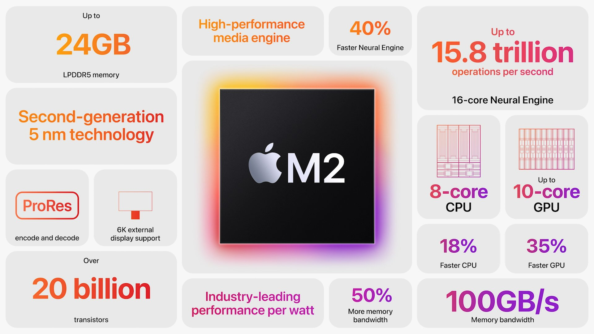
The Apple M2 is a System on a Chip (SoC) from Apple that is found in the late 2022 MacBook Air and, MacBook Pro 13. It offers 8 cores divided in four performance cores and four power-efficiency cores. The big cores offer 192 KB instruction cache, 128 KB data cache, and 16 MB shared L2 cache (up from 12 MB). The four efficiency cores are a lot smaller and offer only 128 KB instruction cache, 64 KB data cache, and 4 MB shared cache. The efficiency cores (E cluster) clock with up to 2,4 GHz, the performance cores (P cluster) with up to 3,5 GHz and therefore higher than the M1 cores. The architecture should be similar to the A15 (iPhone 13) with Avalanche and Blizzard cores.
The chip features a unified memory architecture for the CPU and GPU cores and supports up to 24 GB LPDDR5-6400 for a bandwidth of up to 100GB/s.
According to Apple, the M2 offers a 18% higher CPU performance at the same power consumption level compared to the Apple M1. In our tests, the MacBook Pro 13 with active cooling was able to reach the 18% in Geekbench Multi. In other benchmarks we measured 12 to 15% gains compared to the M1. Therefore, the performance is now near the M1 Pro with 8 cores. The passively cooled MacBook Air may however suffer from throttling in longer load scenarios.
Furthermore, the SoC integrates a fast 16 core neural engine with a peak performance of 16 TOPS (for AI hardware acceleration), a secure enclave (e.g., for encryption), Thunderbolt / USB 4 controller, an ISP, and media de- and encoders.
The Apple M2 includes 20 billion transistors (up from the 16 billion of the M1) and is manufactured in the second generation 5nm process at TSMC (most likely N5P). The power consumption is rated at 20W what we also measured under CPU load.
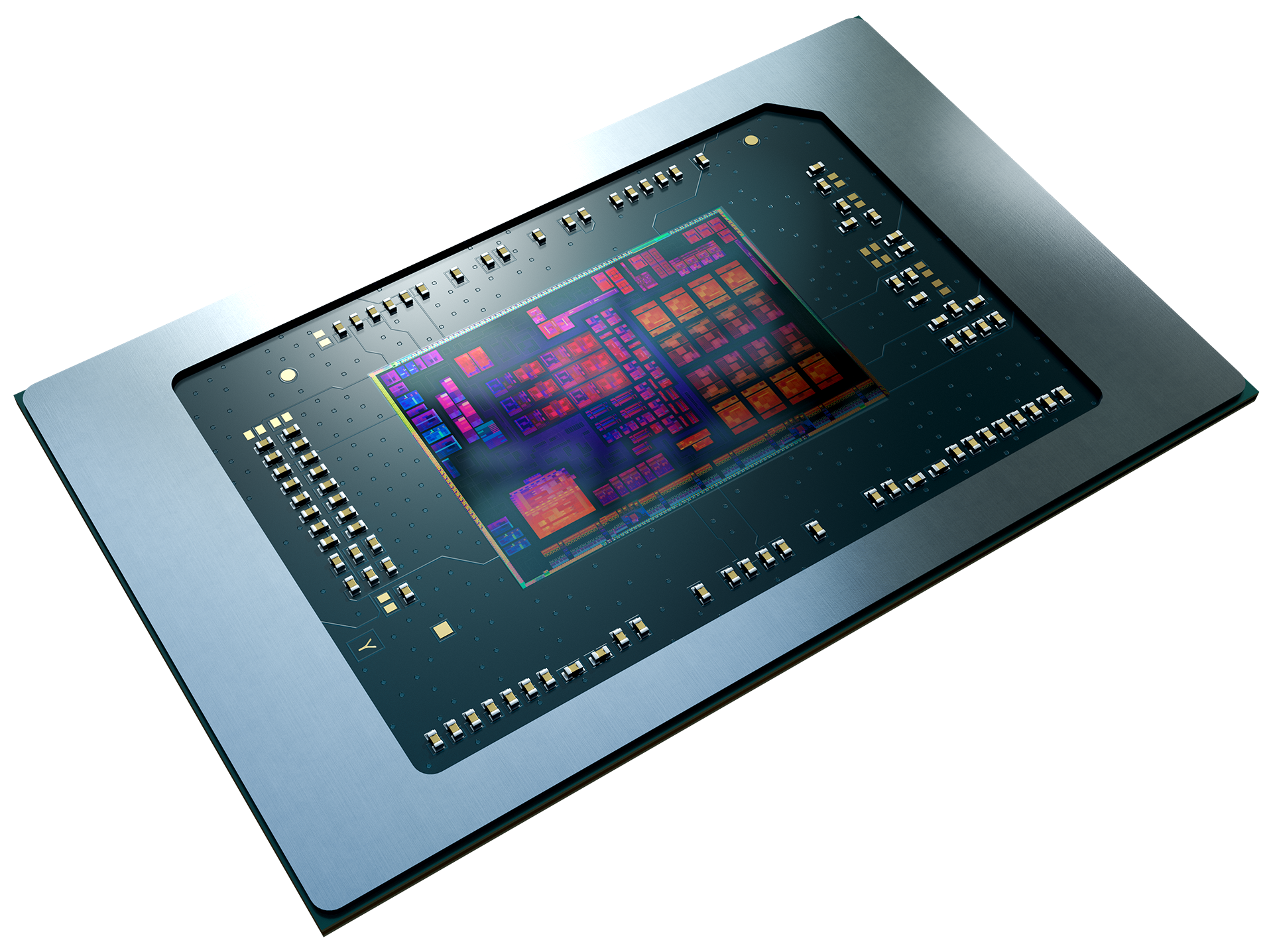
The Ryzen 7 8845HS is a powerful Hawk Point family chip that we believe to be a Ryzen 7 7840HS in disguise. The R7 8845HS was brought to life in H2 2023; it features 8 cores (16 threads thanks to SMT support) running at up to 5.1 GHz. Not only does this APU have full might of the Zen 4 architecture at its disposal, it also boasts the 2nd generation Ryzen AI technology. Last but not the least, the Radeon 780M serves as the integrated GPU.
Architecture & Features
Hawk Point family chips are powered by the Zen 4 architecture, much like Phoenix and Dragon Range family chips are. That's not to say that there is no difference between the three. With Hawk Point, AMD uncorks its 2nd generation Ryzen AI technology meaning the new processors are expected to deliver an up to 40% increase in generative AI performance over 7040 series APUs. Dozens of popular apps such as DaVinci Resolve support this technology, as of late 2023.
Unlike Zen 3, Zen 4 features AVX512 support and, thanks to a plethora of other improvements including larger caches/registers/buffers across the board, is slated to bring a double-digit IPC improvement over the former.
Elsewhere, the 8845HS has 16 MB of L3 cache and a seriously fast RAM controller (up to LPDDR5x-7500 and up to DDR5-5600, ECC-enabled memory included). PCI-Express speeds are capped at 1.97 GB/s per lane which corresponds to the 4.0 spec.
This Ryzen 7 series chip is designed to run 64-bit Windows 11, 64-bit Windows 10 or Linux; please note that it isn't overclockable and neither is it user-replaceable. It gets soldered to the motherboard for good instead (FP7, FP7r2, FP8 socket interfaces).
Performance
Since the 8845HS is a 7840HS in disguise, it's safe to expect it to be just slightly faster than the Core i9-13900H and also the Ryzen 9 7940HS, as far as multi-thread performance is concerned. This is a very fast chip, as of Q3 2023.
Your mileage may vary depending on how high the CPU power limits are and how competent the cooling solution of your system is.
Graphics
The Radeon 780M (12 CUs / 768 shaders, up to 2,700 MHz) is capable of powering 4 monitors simultaneously with resolutions as high as SUHD 4320p. It will also have little issue hardware-encoding and hardware-decoding the most widely used video codecs (AV1, HEVC, AVC). As far as gaming is concerned, the thing will let you play most games at 1080p as long as you are fine with moderate quality settings. Long story short, this is the best iGPU money can buy, as of H2 2023.
Your mileage may vary depending on how high the CPU power limits are, how competent the cooling solution of your system is, how fast the RAM of your system is (there is no dedicated VRAM here).
Power consumption
This Ryzen 7 series chip has a long-term power limit (default TDP) of 35 W to 54 W, giving system makers a choice between improving battery life and making the system they're designing insanely fast. Either way, an active cooling solution is a must for a laptop or a mini-PC built around this APU.
The R7 8845HS is built with a 4 nm TSMC process for high, as of late 2023, energy efficiency.
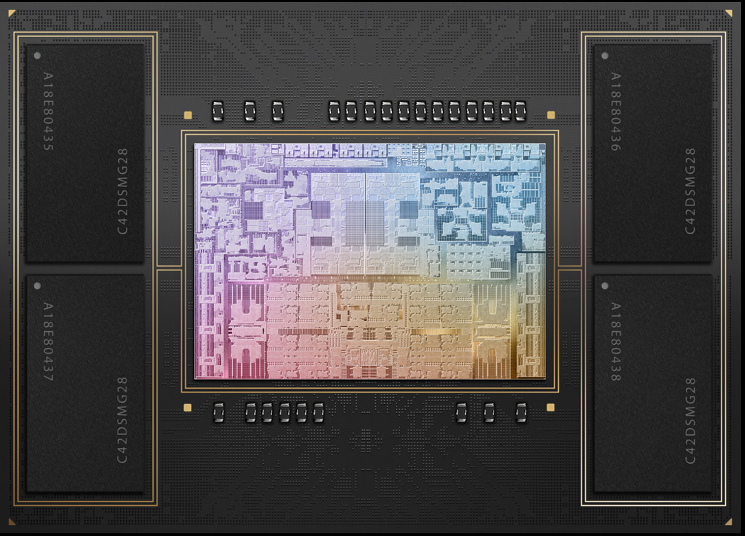
The Apple M2 Pro is a System on a Chip (SoC) from Apple that is found in the early 2023 MacBook Pro 14 and 16-inch models. It offers all 12 cores available in the chip divided in eight performance cores (P-cores) and four power-efficiency cores (E-cores). The E-cores clock with up to 3.4 GHz, the P-Cores up to 3.7 GHz (mostly 3.3 GHz in multi-threaded workloads and 3.4 GHz in single threaded).
The big cores (codename Avalanche) offer 192 KB instruction cache, 128 KB data cache, and 36 MB shared L2 cache (up from 24 MB in the M1 Pro). The four efficiency cores (codename Blizzard) are a lot smaller and offer only 128 KB instruction cache, 64 KB data cache, and 4 MB shared cache. CPU and GPU can both use the 24 MB SLC (System Level Cache).
The unified memory (16 or 32 GB LPDDR5-6400) next to the chip is connected by a 256 Bit memory controller (200 GB/s bandwidth) and can be used by the GPU and CPU.
Apple states that the M2 Pro has a 25% higher performance than the M1 Pro in Xcode compiling.
The integrated graphics card in the M1 Pro offers all 19 cores.
Furthermore, the SoC integrates a fast 16 core neural engine (faster than M1 Pro), a secure enclave (e.g., for encryption), a unified memory architecture, Thunderbolt 4 controller, an ISP, and media de- and encoders (including ProRes).
The M2 Pro is manufactured in 5 nm at TSMC (second generation) and integrates 40 billion transistors.
- Range of benchmark values for this graphics card - Average benchmark values for this graphics card * Smaller numbers mean a higher performance 1 This benchmark is not used for the average calculation
v1.27
log 03. 14:12:00
#0 checking url part for id 14521 +0s ... 0s
#1 checking url part for id 16399 +0s ... 0s
#2 checking url part for id 14973 +0s ... 0s
#3 not redirecting to Ajax server +0s ... 0s
#4 did not recreate cache, as it is less than 5 days old! Created at Sat, 01 Jun 2024 05:37:57 +0200 +0.001s ... 0.001s
#5 composed specs +0.035s ... 0.036s
#6 did output specs +0s ... 0.036s
#7 getting avg benchmarks for device 14521 +0.003s ... 0.039s
#8 got single benchmarks 14521 +0.018s ... 0.057s
#9 getting avg benchmarks for device 16399 +0.019s ... 0.076s
#10 got single benchmarks 16399 +0.017s ... 0.093s
#11 getting avg benchmarks for device 14973 +0.003s ... 0.096s
#12 got single benchmarks 14973 +0.009s ... 0.105s
 Deutsch
 English
 Español
 Français
 Italiano
 Nederlands
 Polski
 Português
 Русский
 Türkçe
 Svenska
 Chinese
 Magyar