Samsung announces next-gen UFS 4.0-based storage for the mobile devices of the future
Currently, OEMs looking to hammer the premium appeal of its new smartphones or tablets home might advertise them in terms of internal storage rated for UFS 3.1 speeds, meaning it meets the latest JEDEC standards for universal flash storage (UFS) quality and speed at the time of their manufacture. However, this buzzword has now been supplanted by a new one, UFS 4.0, and Samsung has confirmed that it can offer storage that meets these criteria.
The South Korean electronics giant has indeed announced new UFS chips with the most up-to-date JEDEC-approved specs. They include a bandwidth that may go as high as 23.2 gigabits per second (Gb/s) per lane of memory, or twice that under UFS 3.1.
This speed is to facilitated by cutting-edge 7th-gen, 176-layer V-NAND, which will come with an in-house controller in Samsung's version of UFS 4.0 storage. The OEM touts it as capable of advanced 4,200 megabyte per second (MB/s) sequential read speeds, not to mention sequential write speeds of up to 2,800MB/s.
These new UFS chips are also already backed to be more power-efficient than ever before, with an estimated sequential read speed of 6MB/s per milllamp (mA), a saving of 46% compared to their predecessors.
Therefore, Samsung asserts that they are more than capable of boosting internal memory performance in next-gen mobile devices, and are also rated for implementions such as 5G use or distribution, extended reality (XR) or next-gen smart vehicles.
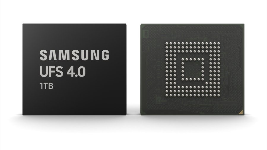
The OEM currently projects that this next-gen UFS 4.0 storage will be in mass production by the third quarter of 2022, at which point they will be made as markedly thin and small (~11 x 13 x 1 millimeters (mm)) individual chips that go up to 1 terabyte (1TB) in capacity.
Source(s)
