

AMD Ryzen 7 3700U vs AMD Ryzen 5 7520U vs AMD Ryzen 5 3580U
AMD Ryzen 7 3700U
► remove from comparisonThe AMD Ryzen 7 3700U is a mobile SoC that was announced in January 2019. It combines four Zen+ cores (8 threads) clocked at 2.3 GHz to 4 GHz with a Radeon RX Vega 10 graphics adapter with 10 CUs (640 shaders) clocked at up to 1,400 MHz. Specified at 15 Watt TDP, the SoC is intended for thin mid-range laptops. In Chromebooks, AMD calles the APU AMD Ryzen 7 3700C, but with the exact same specifications (and performance).
The Picasso SoCs use the Zen+ microarchitecture with slight improvements that should lead to a 3% IPC (performance per clock) improvements.
The integrated dual-channel memory controller supports up to DDR4-2400 memory. As the features of the Picasso APUs are the same compared to the Raven Ridge predecessors, we point to our Raven Ridge launch article.
Performance
The average 3700U in our database is a solid mid-range CPU as of early 2021, its multi-thread benchmark scores matching those of the Core i5-10310U and the Core i5-1035G7 (the Ryzen 5 PRO 3500U is found close nearby as well). This Ryzen 7 is good for more than just binge-watching Netflix and writing e-mails. Just do not expect it to be as fast as a Core i7-11800H.
Thanks to its decent cooling solution and sufficiently high CPU power limits, the ThinkPad E595 is among the fastest laptops powered by the 3700U that we know of. It can be up to 50% faster in CPU-bound workloads than the slowest system featuring the same chip in our database, as of August 2023.
Power consumption
This Ryzen 7 series chip has a default TDP of 15 W (also known as the long-term power limit). This can be changed by a laptop manufacturer to anything between 12 W and 35 W with clock speeds and performance changing accordingly as a result. Either way, that's a little too high to allow for passively cooled designs.
Last but not the least, the Ryzen 7 3700U is manufactured on a 12 nm process for lower-than-average, as of mid-2023, energy efficiency.
AMD Ryzen 5 7520U
► remove from comparison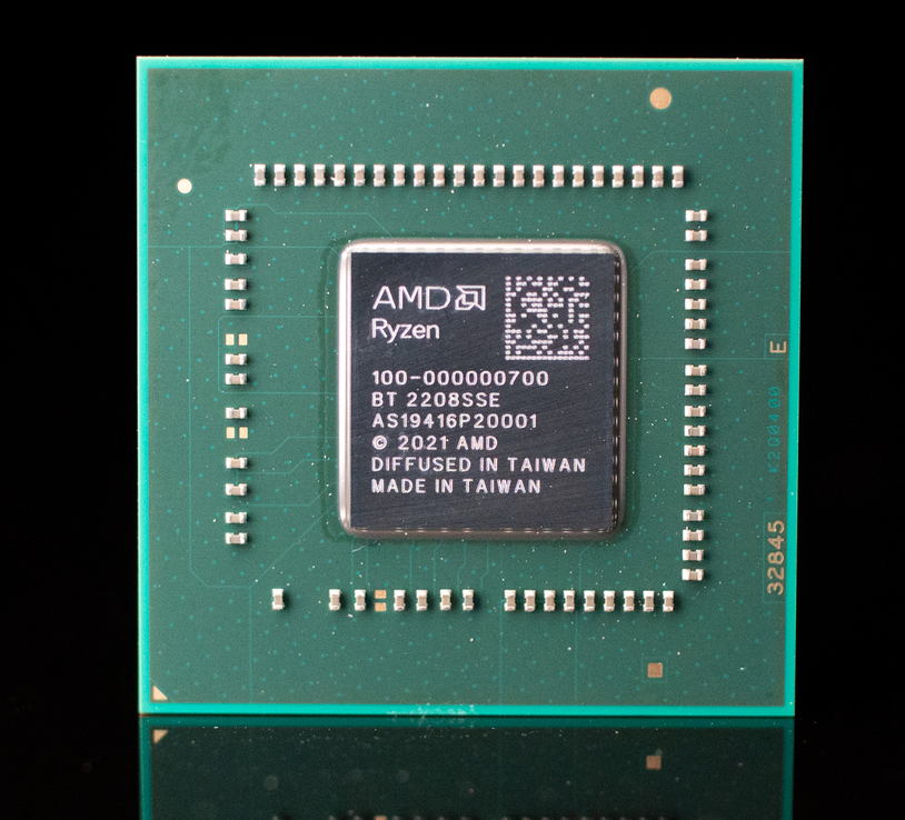
The AMD Ryzen 5 7520U is a mobile processor for cheap laptops of the Mendocino series. It integrates four older Zen 2 cores (similar to the Ryzen 4000 series like the Ryzen 3 4300U). The CPU cores clock from 2.8 GHz (base) to 4.3 GHz (single core Turbo) and can use 4 MB L3 cache. Thanks to SMT/Hyperthreading, the CPU can work on 8 threads simultaneously. The integrated memory controller only supports fast LPDDR5 memory (5500 MHz max.).
The integrated graphics adapter (Radeon 610M iGPU) uses the modern RDNA 2 architecture, but only 2 CUs (128 shaders) and clocks with up to 1.9 GHz.
Performance
The average 7520U in our extensive database is in the same league as the Core i7-1185G7, as far as multi-thread benchmark scores are concerned. This is a so-so result and indicative of a lower mid-range chip, as of Q3 2023.
Your mileage may vary depending on how high the CPU power limits are and how competent the cooling solution of your system is.
Mendocino series chips are produced on a relatively modern 6nm FinFET process at TSMC and should offer a good power efficiency. The R5 7520U is rated at 8-15 W TDP and therefore well suited for thin and light laptops.
AMD Ryzen 5 3580U
► remove from comparisonThe AMD Ryzen 5 3580U, a Microsoft Surface Edition chip, is a mobile SoC that was announced in October 2019 as part of the Surface Book 15. It combines four Zen+ cores (8 threads) clocked at 2.2 - 3.8 GHz with a Radeon RX Vega 9 graphics adapter with 9 CUs (576 Shaders) clocked at up to 1300 MHz. Compared to the similar Ryzen 5 3500U, the 3580 integrates a faster GPU with 9 instead of 8 CUs.
The Picasso SoCs use the Zen+ microarchitecture with slight improvements that should lead to a 3% IPS (performance per clock) improvements. Furthermore, the 12nm process allows higher clock rates at similar power consumptions.
The integrated dual-channel memory controller supports up to DDR4-2400 memory. As the features of the Picasso APUs are the same compared to the Raven Ridge predecessors, we point to our Raven Ridge launch article.
Performance
The average 3580U in our extensive database is in the same league as the Core i5-1035G7 and also the Core i7-10510U, as far as multi-thread benchmark scores are concerned. This is a fairly decent result, as of mid 2021.
Power consumption
This Ryzen 5 has a default TDP (also known as the long-term power limit) of 15 W, a value that laptop manufacturers - or should we say, Microsoft - are allowed to change to anything between 12 W and 35 W with clock speeds and performance changing correspondingly. Those values are not low enough to allow for fan-free designs, for better or worse.
The CPU is built with a fairly old, as of late 2022, 12 nm process for lower-than-average energy efficiency.
| Model | AMD Ryzen 7 3700U | AMD Ryzen 5 7520U | AMD Ryzen 5 3580U | ||||||||||||||||||||||||||||||||||||||||||||||||||||||||
| Codename | Picasso-U (Zen+) | Mendocino-U (Zen 2) | Picasso-U (Zen+) | ||||||||||||||||||||||||||||||||||||||||||||||||||||||||
| Series | AMD Picasso (Ryzen 3000 APU) | AMD Mendocino (Zen 2, Ryzen 7020) | AMD Picasso (Ryzen 3000 APU) | ||||||||||||||||||||||||||||||||||||||||||||||||||||||||
| Series: Picasso (Ryzen 3000 APU) Picasso-U (Zen+) |
|
|
| ||||||||||||||||||||||||||||||||||||||||||||||||||||||||
| Clock | 2300 - 4000 MHz | 2800 - 4300 MHz | 2100 - 3700 MHz | ||||||||||||||||||||||||||||||||||||||||||||||||||||||||
| L1 Cache | 384 KB | 256 KB | 384 KB | ||||||||||||||||||||||||||||||||||||||||||||||||||||||||
| L2 Cache | 2 MB | 2 MB | 2 MB | ||||||||||||||||||||||||||||||||||||||||||||||||||||||||
| L3 Cache | 4 MB | 4 MB | 4 MB | ||||||||||||||||||||||||||||||||||||||||||||||||||||||||
| Cores / Threads | 4 / 8 | 4 / 8 | 4 / 8 | ||||||||||||||||||||||||||||||||||||||||||||||||||||||||
| TDP | 15 Watt | 15 Watt | 15 Watt | ||||||||||||||||||||||||||||||||||||||||||||||||||||||||
| Transistors | 4500 Million | 4500 Million | |||||||||||||||||||||||||||||||||||||||||||||||||||||||||
| Technology | 12 nm | 6 nm | 12 nm | ||||||||||||||||||||||||||||||||||||||||||||||||||||||||
| max. Temp. | 105 °C | 105 °C | |||||||||||||||||||||||||||||||||||||||||||||||||||||||||
| Socket | FP5 | FP5 | |||||||||||||||||||||||||||||||||||||||||||||||||||||||||
| Features | DDR4-2400, PCIe 3, MMX, SSE, SSE2, SSE3, SSSE3, SSE4A, SSE4.1, SSE4.2, AVX, AVX2, BMI2, ABM, FMA, ADX, SMEP, SMAP, SMT, CPB, AES-NI, RDRAND, RDSEED, SHA, SME | LPDDR5-5500 RAM, PCIe 3, MMX (+), SSE, SSE2, SSE3, SSSE3, SSE4.1, SSE4.2, SSE4A, AES, AVX, AVX2, FMA3, SHA | DDR4-2400 RAM, PCIe 3, MMX (+), SSE, SSE2, SSE3, SSSE3, SSE4.1, SSE4.2, SSE4A, AES, AVX, AVX2, FMA3, SHA | ||||||||||||||||||||||||||||||||||||||||||||||||||||||||
| iGPU | AMD Radeon RX Vega 10 ( - 1400 MHz) | AMD Radeon 610M ( - 1900 MHz) | AMD Radeon RX Vega 9 ( - 1300 MHz) | ||||||||||||||||||||||||||||||||||||||||||||||||||||||||
| Architecture | x86 | x86 | x86 | ||||||||||||||||||||||||||||||||||||||||||||||||||||||||
| Announced | |||||||||||||||||||||||||||||||||||||||||||||||||||||||||||
| Manufacturer | www.amd.com | www.amd.com | www.amd.com |

Benchmarks

Average Benchmarks AMD Ryzen 7 3700U → 100% n=15
Average Benchmarks AMD Ryzen 5 7520U → 141% n=15
Average Benchmarks AMD Ryzen 5 3580U → 116% n=15
* Smaller numbers mean a higher performance
1 This benchmark is not used for the average calculation