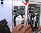
Even though the Nintendo Switch 2 is still many weeks away from hitting shelves, internet sleuths have already managed to get their hands on one and even begun tearing it down. X user @KrunalSalts, famous for their impeccable chip teardowns, has now confirmed a few key Nintendo Switch 2 details.
The Nintendo Switch uses Nvidia's Tegra T239 SoC. It comes with an Arm Cortex X1 core, three Cortex A78 cores, and four Cortex A55 cores, combined with a custom Ampere-based GPU. Next to it, we can see what appear to be two LPDDR modules. This motherboard looks a lot like the one showed by an earlier leak. It also shows a 256 GB UFS 3.1 module from SK Hynix and what could be a Wi-Fi chip from MediaTek.
Krunal says a deeper dive will arrive in the coming days. This will solve one of the biggest mysteries surrounding the Nintendo Switch 2's SoC: which process node is it based on. Because its GPU is Ampere-based, many speculate it was made on Samsung's 8 nm node. However, there are many state it uses a newer 5 nm variant.


