Exynos 2400, 2200, 2100 die shots highlight the chips’ evolution over the years
Samsung's Exynos chips have caught somewhat of a bad rep due to their inability to perform on par with Qualcomm counterparts. While the Exynos 2400 is finally able to trade blows with the Snapdragon 8 Gen 3 in some capacity, the Exynos 2200 and Exynos 2100 were noticeably slower. X user @krunalsalts has now posted die shots of the three chips, highlighting how they've changed over the years unlike Apple's designs, which have largely remained the same. The user has also posted an excellent, in-depth breakdown of the TSMC's N3B node using an Apple A17 Pro on their YouTube channel.
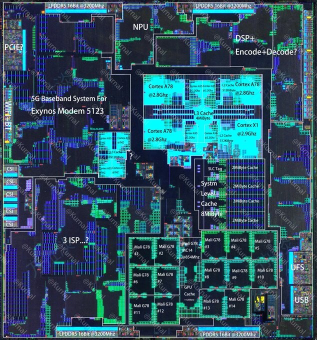
Starting with 2022's Exynos 2100, the 8-core CPU (1x Cortex-X1 + 3x Cortex-A78 + 4x Cortex-A55) and 12-core Arm Mali-G78 GPU take up a good chunk of the die space. The DSP and NPU are crammed above the CPU, while the Exynos 5123 5G modem is next to it. The modem also gets a small cluster of Cortex-A55 cores, which is interesting because the job can easily be done by a lower power Cortex A/M CPU. Lastly, the ISP is located next to the GPU block. Die space was probably not a concern because the chip has an area of 128.09 mm2.
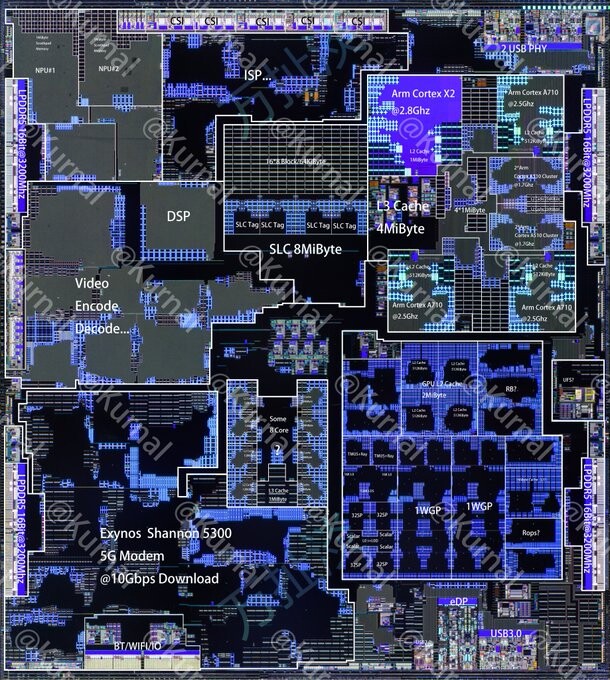
Measuring just 104.65 mm2, the Exynos 2200, received a massive reduction in die area, presumably due to yield issues with the Samsung 4LPE node. This limitation may have promoted Samsung to redesign its internals completely, as is apparent in the photo. The DSP + NPU block was moved next to the CPU, but the 5G modem stayed put. Like its predecessor, the Exynos 5300 5G modem gets 8 low-power Arm CPUs to do the heavy lifting. Furthermore, the RDNA 2-based Xclipse 920 GPU is remarkably smaller than its Arm counterpart.
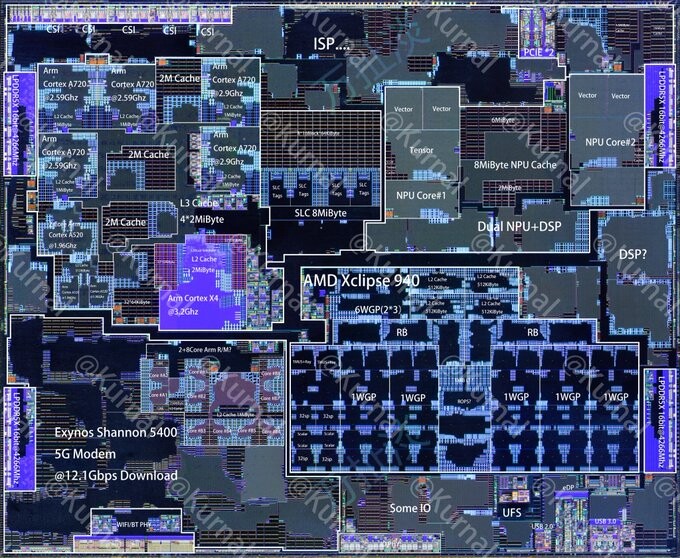
With the Exynos 2300's cancellation, Samsung had quite some time on its hand to develop the Exynos 2400. It, too, got a complete makeover, and this time, Samsung had more room to play with. The Exynos 2400 is the largest chip of the lot with an area of 137.44 mm2. It may have been necessary because the Xclipse 940 GPU featured 6 WGPs (vs 2 on the 920). Plus, it also came with a 10-core CPU, which you can see been relocated once again. Even the NPU has become remarkably larger to accommodate all the advertised on-device AI features.
It'll be interesting to see how the Exynos 2500 looks on the inside. Based on what we know so far, it is more or less identical to the Exynos 2400, at least on the CPU front. This time around, Samsung will be able to fit a lot more components in a tighter space due to the chip being manufactured on the company's MBCFET 3GAP node, whereas its last-gen counterparts used FinFET designs.