

Intel Core i5-12600H vs AMD Ryzen 5 5625U
Intel Core i5-12600H
► remove from comparisonThe Intel Core i5-12600H is a high-end mobile CPU for laptops based on the Alder Lake architecture. It was announced in early 2022 and offers 4 of the 6 performance cores (P-cores, Golden Cove architecture) and all 8 efficient cores (E-cores, Gracemont architecture). The P-cores support Hyper-Threading leading to 16 supported threads when combined with the E-cores. The clock rate ranges from 2.7 to 4.5 GHz on the performance cluster and 2 to 3.3 GHz on the efficient cluster. The performance of the E-cores should be similar to old Skylake cores (compare to the Core i7-6700HQ). All cores can use up to 18 MB L3 cache. Compared to the 12650H, the 12600H offers less P-cores but more E-cores, a faster iGPU and "Enterprise" vPro features (for remote management).
Performance
Thanks to the 12 cores, the multi-threaded performance should be clearly faster than the older Tiger Lake-H CPUs with similar clock speeds (especially like the Core i5-11500H with only 6 cores). Due to the architectural improvements, single-core performance is also better than similar or higher clocked Tiger Lake CPUs.
Features
The integrated memory controller supports various memory types up to DDR5-4800, DDR4-3200, LPDDR5-5200, and LPDDR4x-4267. The Thread Director (in hardware) can support the operating system to decide which thread to use on the performance or efficient cores for the best performance. For AI tasks, the CPU also integrates GNA 3.0 and DL Boost (via AVX2). Quick Sync in version 8 is the same as in the Rocket Lake CPUs and supports MPEG-2, AVC, VC-1 decode, JPEG, VP8 decode, VP9, HEVC, and AV1 decode in hardware. The CPU only supports PCIe 4.0 (x8 for a GPU and two x4 for SSDs).
The integrated graphics card is based on the Xe-architecture and offers 80 of the 96 EUs (Execution Units) operating at up to 1.4 GHz.
The CPU is rated at 45 W base power (95 W PL2) but most laptops will use a PL1 of around 60 Watt. The SoC is manufactured in a 10nm process at Intel, which is known as Intel 7.
AMD Ryzen 5 5625U
► remove from comparison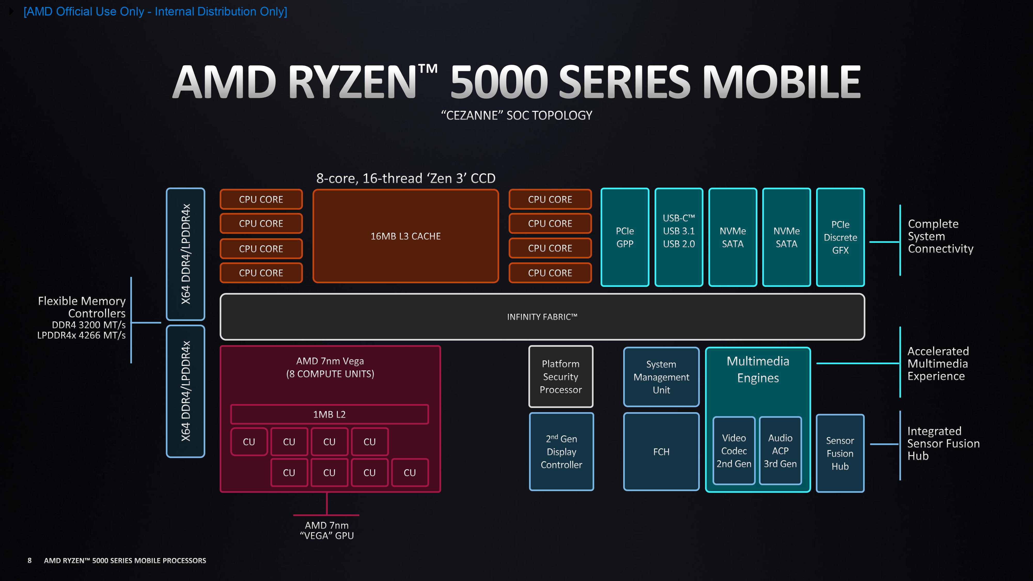
The AMD Ryzen 5 5625U is a processor for thin and light laptops based on the Cezanne generation. It is part of the "Barcelo" refresh in early 2022 and offers 100 MHz higher boost clock for the CPU cores compared to the old Ryzen 5 5600U. The R5 5625U integrates six of the eight cores based on the Zen 3 microarchitecture and is the third fastest U-5000-series processor at launch. The cores are clocked at 2.3 (guaranteed base clock) to 4.3 GHz (Turbo) and support SMT for a total of 12 threads. The chip is manufactured on the modern 7 nm TSMC process.
In addition to the six CPU cores, the APU also integrates a Radeon RX Vega 7 integrated graphics card with 7 CUs at up to 1800 MHz. The dual channel memory controller supports DDR4-3200 and energy efficient LPDDR4-4266 RAM. Furthermore, 16 MB level 3 cache (up from 8 MB at the 4800U) can be found on the chip.
Performance
The average 5625U in our database is in the same league as the Core i5-1255U, Core i5-1335U, Core i5-1345U and also the Ryzen 5 7530U, as far as multi-thread benchmark scores are concerned. This is a decent result, as of Q3 2023.
Your mileage may vary depending on how high the CPU power limits are and how competent the cooling solution of your system is.
Power consumption
This Ryzen has a default TDP of 15 W (also known as the Power Limit 1). Which is a little too high to allow for passively cooled designs.
The APU is built with TSMC's 7 nm process for higher-than-average, as of mid-2022, energy efficiency.
| Model | Intel Core i5-12600H | AMD Ryzen 5 5625U | ||||||||||||||||||||||||||||||||||||||||||||
| Codename | Alder Lake-H | Barcelo-U (Zen 3) | ||||||||||||||||||||||||||||||||||||||||||||
| Series | Intel Alder Lake-P | AMD Cezanne (Zen 3, Ryzen 5000) | ||||||||||||||||||||||||||||||||||||||||||||
| Series: Cezanne (Zen 3, Ryzen 5000) Barcelo-U (Zen 3) |
|
| ||||||||||||||||||||||||||||||||||||||||||||
| Clock | 2000 - 4500 MHz | 2300 - 4300 MHz | ||||||||||||||||||||||||||||||||||||||||||||
| L1 Cache | 1.1 MB | 384 KB | ||||||||||||||||||||||||||||||||||||||||||||
| L2 Cache | 10 MB | 3 MB | ||||||||||||||||||||||||||||||||||||||||||||
| L3 Cache | 18 MB | 16 MB | ||||||||||||||||||||||||||||||||||||||||||||
| Cores / Threads | 12 / 16 | 6 / 12 | ||||||||||||||||||||||||||||||||||||||||||||
| TDP | 45 Watt | 15 Watt | ||||||||||||||||||||||||||||||||||||||||||||
| Technology | 10 nm | 7 nm | ||||||||||||||||||||||||||||||||||||||||||||
| max. Temp. | 100 °C | 95 °C | ||||||||||||||||||||||||||||||||||||||||||||
| Socket | BGA1744 | FP6 | ||||||||||||||||||||||||||||||||||||||||||||
| Features | DDR4-3200/LPDDR4x-4266/DDR5-4800/LPDDR5-5200 RAM, PCIe 4, Thr. Dir., DL B,., GNA, vPro En., RPE, MMX, SSE, SSE2, SSE3, SSSE3, SSE4.1, SSE4.2, AVX, AVX2, BMI2, ABM, FMA, ADX, VMX, SMX, SMEP, SMAP, EIST, TM1, TM2, HT, Turbo, SST, AES-NI, RDRAND, RDSEED, SHA | DDR4-3200/LPDDR4x-4266 RAM (incl. ECC), PCIe 3, MMX, SSE, SSE2, SSE3, SSSE3, SSE4A, SSE4.1, SSE4.2, AVX, AVX2, BMI2, ABM, FMA, ADX, SMEP, SMAP, SMT, CPB, AES-NI, RDRAND, RDSEED, SHA, SME | ||||||||||||||||||||||||||||||||||||||||||||
| iGPU | Intel Iris Xe Graphics G7 80EUs ( - 1400 MHz) | AMD Radeon RX Vega 7 ( - 1800 MHz) | ||||||||||||||||||||||||||||||||||||||||||||
| Architecture | x86 | x86 | ||||||||||||||||||||||||||||||||||||||||||||
| Announced | ||||||||||||||||||||||||||||||||||||||||||||||
| Manufacturer | ark.intel.com | www.amd.com |

Benchmarks
Average Benchmarks AMD Ryzen 5 5625U → 0% n=0
* Smaller numbers mean a higher performance
1 This benchmark is not used for the average calculation