

Intel Core Ultra 7 255U vs Intel Core i7-12700F vs Intel Core i5-12600K
Intel Core Ultra 7 255U
► remove from comparisonThe Intel Core Ultra 7 255U is an upper mid-range CPU with 12 cores from the Arrow Lake U series, which was introduced at the beginning of 2025. The chip is similar to the Meteor Lake U series, but the compute part is manufactured using the modern Intel 3 process and therefore offers higher clock rates.
Like its predecessor, the SoC is based on a tile/chiplet design. The smaller compute tile (compared to the H processors) offers 2 performance cores (P cores, Redwood Cove architecture, SMT) and 8 efficiency cores (E cores, Crestmont architecture). The P-cores support hyperthreading (therefore 14 threads together) and clock up to 5.2 GHz. The E-cores clock at a maximum of 4.2 GHz. In addition, there are now two more low-power efficiency cores with up to 2.4 GHz on the low-power island; the compute tile can therefore be completely deactivated when idle and during simple tasks in order to save power.
Performance
Due to the higher clock rates, the Core Ultra 7 255U can clearly distinguish itself from the old top model Core Ultra 7 165U (12 cores, max 4.9 / 3.8 GHz, 12 MB cache). The old Core Ultra 7 155U lags even further behind due to its low clock rates.
Graphics unit
The Core Ultra 7 155U offers a new Arc-based iGPU called Intel Graphics with 4 Xe cores and 64 EUs that reach a maximum of 2.1 GHz. However, the performance is far below the new Arc iGPU in the H series.
Features
Arrow Lake-U has integrated WiFi 6E (WiFi 7 optional). The integrated memory controller now supports LPDDR5/x-8400 or DDR5-6400 (max. 128 GB). A dedicated NPU (2x Gen3 Neural Compute Engines) is now used. The Xe Media Engine supports MPEG-2, AVC, VC-1 Decode, JPEG, VP8 Decode, VP9, HEVC and AV1 Decode up to 8K 10-bit HDR. The chip now supports PCIe-5.0 (x8 for GPU) and PCIe-4.0 (three x12 for SSDs).
Power consumption
The Intel Core Ultra 7 255U is specified with 15 watts TDP (base) and 57 watts (PL2) max. turbo power. Meteor Lake consists of five individual chips, whereby the processor part is manufactured in the new Intel 3 process (5nm). The graphics unit is produced at TSMC in N5 and the SoC and I/O tile in the older N6 process. These 4 chips are then applied to the 22nm base tile using the Foveros process.
Intel Core i7-12700F
► remove from comparisonThe Intel Core i7-12700F is a high end CPU for desktops based on the Alder Lake architecture. It was first announced in November 2021 and offers 8 performance cores and 4 efficiency cores. The performance cores (P-cores) support HyperThreading, leading to 20 threads that can be processed at once. The performance cores can clock with up to 4.9 GHz (Turbo Boost Max 3.0, 2.1 base), the efficiency cores can clock with up to 3.6 GHz (1.6 GHz base). All cores can use 25 MB Smart Cache. The integrated memory controller supports up to 128 GB DDR5 with 4800 MT/s (dual channel).
The Thread Director (in hardware) can support the operating system to decide which thread to use on the performance or efficiency cores for the best performance.
For AI tasks, the CPU also integrates GNA 3.0 and DL Boost. Quick Sync in version 8 is the same as in the Rocket Lake CPUs and supports MPEG-2, AVC, VC-1 decode, JPEG, VP8 decode, VP9, HEVC and AV1 decode in hardware.
The F-series desktop models don't offer an integrated graphics card.
The CPU is rated at 65 W base power and 180 Watt maximum Turbo power. It is manufactured in 10nm, called Intel 7, process at Intel.
Intel Core i5-12600K
► remove from comparison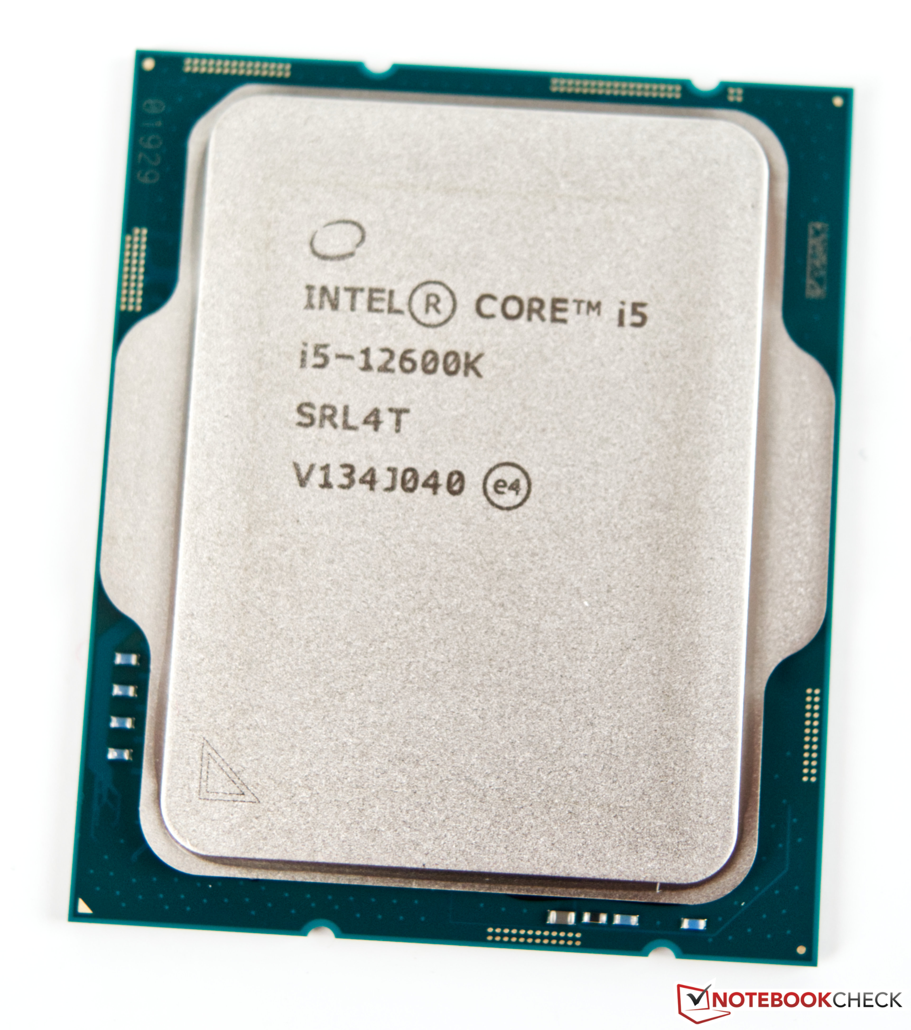
The Intel Core i5-12600K is a mid-range CPU for desktops based on the Alder Lake architecture. It was first announced in November 2021 and offers 6 performance cores and 4 efficiency cores. The performance cores (P-cores) support HyperThreading, leading to 16 Threads that can be processed at once. The performance cores can clock with up to 4.9 GHz, the efficiency cores can clock with up to 3.6 GHz. All cores can use 20 MB Smart Cache. The integrated memory controller supports up to 128 GB DDR5 with 4800 MT/s (dual channel).
Thread Director (in hardware) can support the operating system to decide which thread to use on the performance or efficiency cores for the best performance.
The integrated graphics adapter is based on the Xe-architecture and called Intel UHD Graphics 770. It clocks between 300 and 1.45 GHz.
For AI tasks, the CPU also integrates GNA 3.0 and DL Boost. Quick Sync in version 8 is the same as in the Rocket Lake CPUs and supports MPEG-2, AVC, VC-1 decode, JPEG, VP8 decode, VP9, HEVC and AV1 decode in hardware.
Performance
The average 12600K in our database is way ahead of the Ryzen 9 3900 and the Core i9-10900K, as far as multi-thread benchmark scores are concerned. This is a very fast CPU that should have no trouble running triple-A games for at least a couple of years.
Power consumption
This Core i5 series chip has a Base power consumption of 125 W, with its maximum Intel-recommended Turbo power consumption sitting at 150 W.
The i5-12600K is built with Intel's fourth generation 10 nm process marketed as Intel 7 for lower-than-average, as of mid 2023, energy efficiency.
| Model | Intel Core Ultra 7 255U | Intel Core i7-12700F | Intel Core i5-12600K | ||||||||||||||||||||||||||||||||||||||||||||||||||||||||||||||||
| Codename | Arrow Lake-U | Alder Lake | Alder Lake | ||||||||||||||||||||||||||||||||||||||||||||||||||||||||||||||||
| Series | Intel Meteor Lake-U | Intel Alder Lake-S | Intel Alder Lake-S | ||||||||||||||||||||||||||||||||||||||||||||||||||||||||||||||||
| Series: Alder Lake-S Alder Lake |
|
|
| ||||||||||||||||||||||||||||||||||||||||||||||||||||||||||||||||
| Clock | 3800 - 4800 MHz | 3300 - 4900 MHz | 2800 - 4900 MHz | ||||||||||||||||||||||||||||||||||||||||||||||||||||||||||||||||
| L3 Cache | 12 MB | 25 MB | 20 MB | ||||||||||||||||||||||||||||||||||||||||||||||||||||||||||||||||
| Cores / Threads | 12 / 14 2 x 5.2 GHz Intel Redwood Cove P-Core 8 x 4.2 GHz Intel Crestmont E-Core 2 x 2.4 GHz Intel Crestmont E-Core | 12 / 20 | 10 / 16 | ||||||||||||||||||||||||||||||||||||||||||||||||||||||||||||||||
| TDP | 15 Watt | 65 Watt | 125 Watt | ||||||||||||||||||||||||||||||||||||||||||||||||||||||||||||||||
| Technology | 5 nm | 10 nm | 10 nm | ||||||||||||||||||||||||||||||||||||||||||||||||||||||||||||||||
| max. Temp. | 110 °C | 100 °C | 100 °C | ||||||||||||||||||||||||||||||||||||||||||||||||||||||||||||||||
| Socket | BGA2049 | LGA 1700 | LGA1700 | ||||||||||||||||||||||||||||||||||||||||||||||||||||||||||||||||
| Features | DDR5-6400/LPDDR5-8400/LPDDR5x-8400 RAM, PCIe 4, Thr. Director, DL Boost, AI Boost, vPro Essen., MMX, SSE, SSE2, SSE3, SSSE3, SSE4.1, SSE4.2, AES, AVX, AVX2, AVX-VNNI, FMA3, SHA | DDR4-3200/DDR5-4800 RAM, PCIe 5, Thr. Dir., DL Boost, GNA, vPro Enterp., MMX, SSE, SSE2, SSE3, SSSE3, SSE4.1, SSE4.2, AVX, AVX2, BMI2, ABM, FMA, ADX, SMEP, SMAP, EIST, TM1, TM2, HT, Turbo, SST, AES-NI, RDRAND, RDSEED, SHA | |||||||||||||||||||||||||||||||||||||||||||||||||||||||||||||||||
| iGPU | Intel Graphics 4-Core iGPU (Arc) ( - 2100 MHz) | Intel UHD Graphics 770 (300 - 1450 MHz) | |||||||||||||||||||||||||||||||||||||||||||||||||||||||||||||||||
| Architecture | x86 | x86 | x86 | ||||||||||||||||||||||||||||||||||||||||||||||||||||||||||||||||
| Announced | |||||||||||||||||||||||||||||||||||||||||||||||||||||||||||||||||||
| Manufacturer | ark.intel.com | ark.intel.com | |||||||||||||||||||||||||||||||||||||||||||||||||||||||||||||||||
| L1 Cache | 1 MB | ||||||||||||||||||||||||||||||||||||||||||||||||||||||||||||||||||
| L2 Cache | 12 MB | 9.5 MB | |||||||||||||||||||||||||||||||||||||||||||||||||||||||||||||||||
| Die Size | 215 mm2 | ||||||||||||||||||||||||||||||||||||||||||||||||||||||||||||||||||
| $386 U.S. | $289 U.S. |

Benchmarks
Average Benchmarks Intel Core i7-12700F → 0% n=0
Average Benchmarks Intel Core i5-12600K → 0% n=0
* Smaller numbers mean a higher performance
1 This benchmark is not used for the average calculation