 Deutsch
 English
 Español
 Français
 Italiano
 Nederlands
 Polski
 Português
 Русский
 Türkçe
 Svenska
 Chinese
 Magyar
Intel Processor U300 vs Intel Core 2 Duo T9900 vs Intel Core 2 Duo P8400
Intel Processor U300
► remove from comparison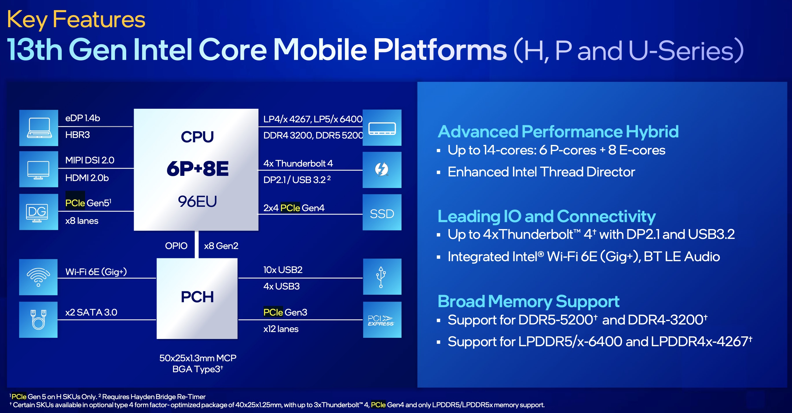
The Intel Processor U300 is an entry-level mobile CPU for thin and light laptops of the Raptor Lake-U series. It was announced in early 2023 and offers one performance core (Raptor Cove architecture P-core, similar to Alder Lake) and 4 efficient cores (E-cores, Gracemont architecture). The P-cores support Hyper-Threading for 6 processing threads when combined with the E-cores. The clock rate ranges from 1.2 to 4.4 GHz on the performance cluster and 0.9 to 3.3 GHz on the efficient cluster. The per-clock performance of the E-cores should be similar to old Skylake cores (compare to the Core i7-6700HQ). All cores have access to 8 MB of L3 cache.
Performance
While we have not tested a single system powered by the U300 as of February 2024, its performance should be very similar to the outgoing Alder Lake Pentium 8505, since there is little difference between the two. The average U300 is set to be 10% to 20% behind the Ryzen 3 5300U and the Core i7-1185G7, as far as multi-thread benchmark scores are concerned, making the former an entry-level chip as of early 2024.
Your mileage may vary depending on how high the CPU power limits are.
Features
The integrated memory controller supports various memory types up to DDR5-4800, DDR4-3200, LPDDR5-5200, and LPDDR4x-4267. The Thread Director (in hardware) can support the operating system to decide which thread to use on the performance or efficient cores for the best performance. For AI tasks, the CPU also integrates GNA 3.0 and DL Boost (via AVX2). Quick Sync in version 8 is the same as in the Rocket Lake CPUs and supports MPEG-2, AVC, VC-1 decode, JPEG, VP8 decode, VP9, HEVC, and AV1 decode in hardware. Several PCIe 4 lanes (x8 for a GPU and two x4 for SSDs) as well as several PCIe 3 lanes are on offer.
The integrated graphics adapter is based on the Xe architecture and offers 48 of the 96 EUs (Execution Units) operating at up to 1.1 GHz.
Power consumption
The U300 has a base power consumption of 15 W, with 55 W being its maximum Intel-recommended Turbo power consumption. The CPU is built with a 10 nm process marketed as Intel 7.
Intel Core 2 Duo T9900
► remove from comparison
The Intel Core 2 Duo T9900 is the theoretical successor of the Core 2 Extreme X9100 (which also clocks at 3.06 GHz) that uses less power due to the modern stepping and the Enhanced Halt State (C1E). The only advantage of the X9100 is the free multiplikator (which allows easy overclocking of the CPU).
The T9900 is a fast dual core CPU for laptops which features 6 MB of shared level 2 cache and a TDP of 35 Watt. Due to the high clock speed, modern games (in 2009) should not be limited by the CPU speed. For single threaded applications it is one of the fastest CPUs for laptops (only beaten by the new Core i7 with enabled Turbo mode).
The T9900 uses a Penryn (Montevina Update) core that features 2 integer units, 1 floating point unit, 1 load unit, and 1 store unit in a 14-stages long pipeline. Due to the Wide Dynamic Execution Technology, the core is able to simultaneously execute up to four instructions.
The integrated Enhanced Speedstep is able to downclock the core dynamically as low as 800 MHz to save power (in idle mode).
The Core 2 Duo T9900 can be used in a Socket P socket with 479 pins: Socket P / Micro Flip-Chip Pin Grid Array (Micro-FCPGA) requires 479-pin surface mount Zero Insertion Force (ZIF) socket (mPGA479M socket) or Micro Flip-Chip Ball Grid Array (Micro-FCBGA) for surface mount (479-ball).
Intel Core 2 Duo P8400
► remove from comparison
The Intel Core 2 Duo P8400 is a dual core processor for laptops. It features 2.26 GHz and a shared level 2 cache of 3 MB. Due to the smaller cache (Core 2 Duo T-Models got usually 6 MB at this clock rate), the TDP is only 25 Watt (instead of the 35 Watt of the T-models).
The performance of the P8400 is on par with the fast Turion II Ultra with about 2.4 to 2.6 GHz. Modern demanding games like Supreme Commander may be limited by the CPU performance. High end gamers should choose a higher clocked Core 2 Duo (or Core i5 / i7).
The P8400 uses a Penryn (Montevina Update) core that features 2 integer units, 1 floating point unit, 1 load unit, and 1 store unit in a 14-stages long pipeline. Due to the Wide Dynamic Execution Technology, the core is able to simultaneously execute up to four instructions.
The integrated Enhanced Speedstep is able to downclock the core dynamically as low as 800 MHz to save power (in idle mode).
The Core 2 Duo P8400 can be used in a Socket P socket with 479 pins: Socket P / Micro Flip-Chip Pin Grid Array (Micro-FCPGA) requires 479-pin surface mount Zero Insertion Force (ZIF) socket (mPGA479M socket) or Micro Flip-Chip Ball Grid Array (Micro-FCBGA) for surface mount (479-ball)
| Model | Intel Processor U300 | Intel Core 2 Duo T9900 | Intel Core 2 Duo P8400 | ||||||||||||||||||||||||||||||||
| Series | Intel Raptor Lake-U | Intel Core 2 Duo | Intel Core 2 Duo | ||||||||||||||||||||||||||||||||
| Codename | Raptor Lake-U | Penryn | Penryn | ||||||||||||||||||||||||||||||||
| Series: Core 2 Duo Penryn |
| ||||||||||||||||||||||||||||||||||
| Clock | 900 - 4400 MHz | 3060 MHz | 2260 MHz | ||||||||||||||||||||||||||||||||
| L1 Cache | 464 KB | 128 KB | 128 KB | ||||||||||||||||||||||||||||||||
| L2 Cache | 3.5 MB | 6 MB | 3 MB | ||||||||||||||||||||||||||||||||
| L3 Cache | 8 MB | ||||||||||||||||||||||||||||||||||
| Cores / Threads | 5 / 6 1 x 4.4 GHz Intel Raptor Cove P-Core 4 x 3.3 GHz Intel Gracemont E-Core | 2 / 2 | 2 / 2 | ||||||||||||||||||||||||||||||||
| TDP | 15 Watt | 35 Watt | 25 Watt | ||||||||||||||||||||||||||||||||
| TDP Turbo PL2 | 55 Watt | ||||||||||||||||||||||||||||||||||
| 10 nm | 45 nm, 1.05-1.2125 V | 45 nm, 1.05-1.15 | |||||||||||||||||||||||||||||||||
| max. Temp. | 100 °C | 105 °C | 105 °C | ||||||||||||||||||||||||||||||||
| Socket | BGA1744 | Socket P (BGA479, PGA478) | Socket P | ||||||||||||||||||||||||||||||||
| Features | DDR4-3200/LPDDR4x-4267/DDR5-5200/LPDDR5-5200/LPDDR5x-5200 RAM, PCIe 4, Thr. Director, DL Boost, GNA, MMX, SSE, SSE2, SSE3, SSSE3, SSE4.1, SSE4.2, AVX, AVX2, BMI2, ABM, FMA, ADX, VMX, SMEP, SMAP, EIST, TM1, TM2, HT, Turbo, SST, AES-NI, RDRAND, RDSEED, SHA | SSE4.1, Virtualization Technology, Execute Disable Bit, Enhanced Speedstep, Ehnaced Halt State (C1E), 64 Bit, Trusted Execution Technology | SSE4.1, Virtualization Technology, Execute Disable Bit, Enhanced Speedstep, Ehnaced Halt State (C1E), 64 Bit, Trusted Execution Technology | ||||||||||||||||||||||||||||||||
| iGPU | Intel UHD Graphics Xe G4 48EUs ( - 1100 MHz) | ||||||||||||||||||||||||||||||||||
| Architecture | x86 | x86 | x86 | ||||||||||||||||||||||||||||||||
| Announced | |||||||||||||||||||||||||||||||||||
| Manufacturer | ark.intel.com | ark.intel.com | ark.intel.com | ||||||||||||||||||||||||||||||||
| FSB | 1066 | 1066 | |||||||||||||||||||||||||||||||||
| Transistors | 410 Million | 410 Million | |||||||||||||||||||||||||||||||||
| Die Size | 107 mm2 | 107 mm2 | |||||||||||||||||||||||||||||||||
| $530 U.S. | $209 U.S. |

