

AMD Ryzen 5 7535HS vs AMD Ryzen 5 PRO 7530U vs AMD Ryzen 3 7335U
AMD Ryzen 5 7535HS
► remove from comparison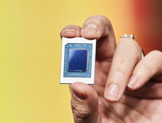
The AMD Ryzen 5 7535HS is a processor for big (gaming) laptops based of the Rembrandt Refresh generation. The R5 7535HS integrates six of the eight cores based on the Zen 3+ microarchitecture. They are clocked at 3.3 (guaranteed base clock) to 4.55 GHz (boost) and support SMT / Hyperthreading (12 threads). The 7535HS is a refresh of the old Ryzen 5 6600HS / 6600H with 50 MHz higher boost clock speed.
The Zen 3+ architecture is a refresh of Zen 3 and should not offer a lot of changes. The chip itself however, offers some modern features, like support for USB 4 (40 Gbps), PCI-E Gen 4 and DDR5-4800MT/s or LPDDR5-6400MT/s.
The processor performance is very similar to the Ryzen 5 6600HS (35 Watt TDP) or Ryzen 5 6600H (55 Watt TDP) due to the similar specs.
In the 6000 series, AMD switched to the RDNA 2 graphics architecture for the iGPU. As the 6600HS the 7535HS only offers the slower Radeon 660M with 6 of the 12 CUs enabled and 1.9 GHz max. clock rate.
The TDP of the APU is specified from 35 to 54 Watt. The monolithic chip is manufactured in 6nm at TSMC.
AMD Ryzen 5 PRO 7530U
► remove from comparison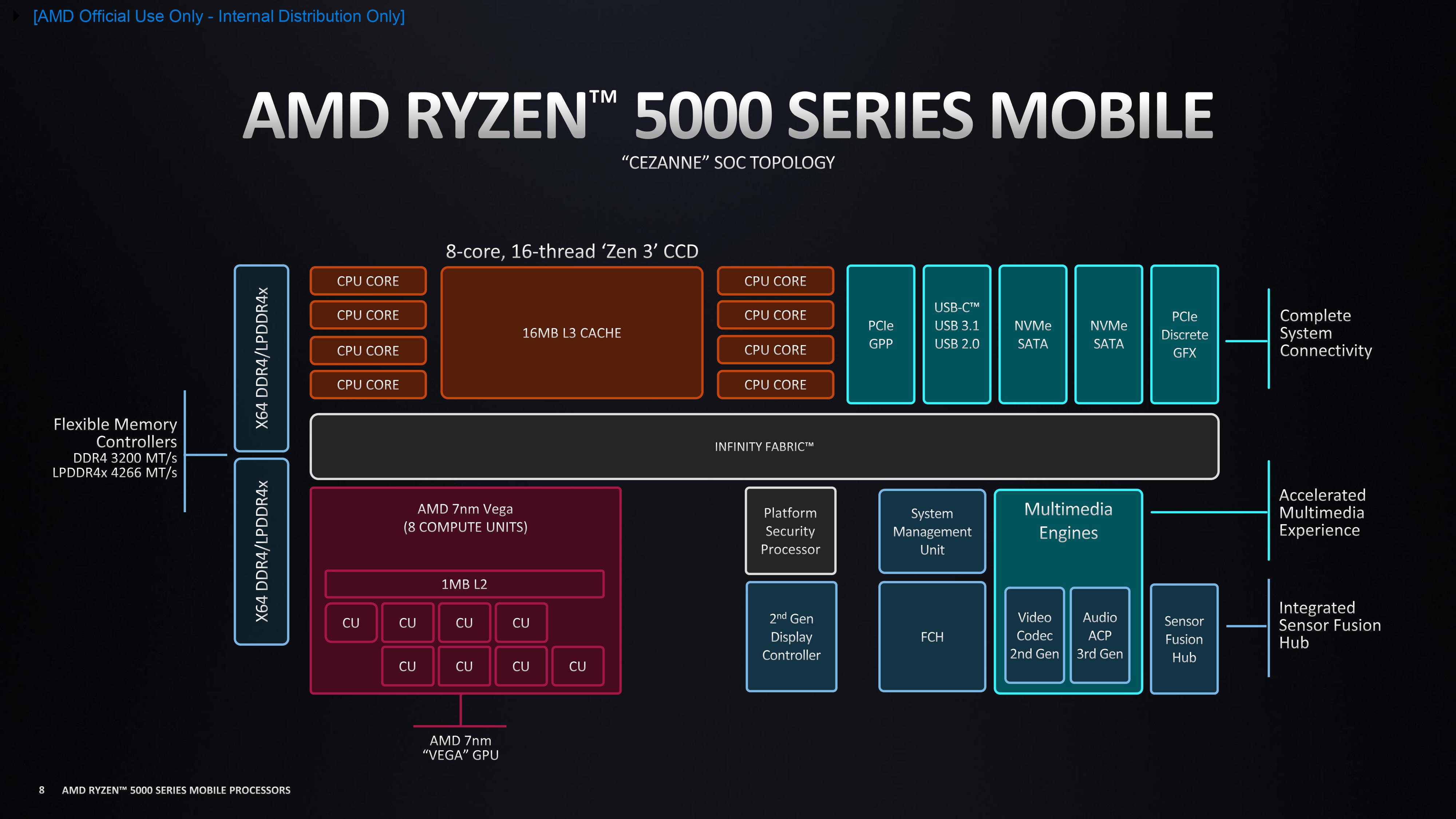
The AMD Ryzen 5 PRO 7530U is a processor for thin and light laptops based on the Cezanne generation. It is part of the second "Barcelo" refresh in early 2023 and offers 200 MHz higher boost clock for the CPU cores compared to the old Ryzen 5 5625U (but a slower base clock speed). The R5 7530U integrates six of the eight cores based on the Zen 3 microarchitecture. The cores are clocked at 2 (guaranteed base clock) to 4.5 GHz (single core boost) and support SMT for a total of 12 threads. The chip is manufactured in 7 nm at TSMC.
Similar to the Ryzen 5 7530U but adding support for "PRO" features like management, security and long term replacement support.
Performance
The average 7530U in our database is in the same league as the Ryzen 5 5625U, Ryzen 7 4800U, Ryzen 7 PRO 5850U, Core i5-1335U, as far as multi-thread benchmark scores are concerned.
In addition to the six CPU cores, the APU also integrates a Radeon RX Vega 7 (now only called Radeon Graphics) integrated graphics card with 7 CUs at up to 2 GHz. The dual channel memory controller supports DDR4-3200 and energy efficient LPDDR4-4266 RAM. Additionally, the chip contains a 16 MB level 3 cache, increased from 8 MB found in the 4800U.
Power consumption
This Ryzen has a default TDP of 15 W (also known as the Power Limit 1).
AMD Ryzen 3 7335U
► remove from comparisonThe AMD Ryzen 3 7335U is a processor for mid-sized laptops based of the Rembrandt refresh generation. The Ryzen packs four of the eight cores based on the Zen 3+ microarchitecture. They are clocked at 3 (guaranteed base clock) to 4.3 GHz (single core boost) and support SMT / Hyperthreading (8 threads). The 7335U is the first Ryzen 3 based on the Zen 3+ architecture and slowest model of the 7035U series.
The Zen 3+ is a refresh of the Zen 3 architecture and should not offer a lot of changes. The chip offers modern features, like support for USB 4 (40 Gbps), PCI-E Gen 4 and DDR5-4800MT/s or LPDDR5-6400MT/s.
The performance should be clearly better than the old Ryzen 3 5300U and Ryzen 3 5425U due to the higher clock speed and improved architecture.
The integrated GPU Radeon 660M is still a fast iGPUs based on the RDNA2 architecture and offers 4 of the 12 CUs at up to 1.8 GHz.
The Ryzen 7335U is manufactured in 6nm FinFET at TSMC and specified at a TDP of 28W.
| Model | AMD Ryzen 5 7535HS | AMD Ryzen 5 PRO 7530U | AMD Ryzen 3 7335U | ||||||||||||||||||||||||||||||||||||||||||||||||||||||||||||||||
| Codename | Rembrandt R | Barcelo-U Refresh | Rembrandt R | ||||||||||||||||||||||||||||||||||||||||||||||||||||||||||||||||
| Series | AMD Rembrandt (Zen 3+) | AMD Cezanne (Zen 3, Ryzen 5000) | AMD Rembrandt (Zen 3+) | ||||||||||||||||||||||||||||||||||||||||||||||||||||||||||||||||
| Series: Rembrandt (Zen 3+) Rembrandt R |
|
|
| ||||||||||||||||||||||||||||||||||||||||||||||||||||||||||||||||
| Clock | 3300 - 4550 MHz | 2000 - 4500 MHz | 3000 - 4300 MHz | ||||||||||||||||||||||||||||||||||||||||||||||||||||||||||||||||
| L1 Cache | 384 KB | 384 KB | 256 KB | ||||||||||||||||||||||||||||||||||||||||||||||||||||||||||||||||
| L2 Cache | 3 MB | 3 MB | 2 MB | ||||||||||||||||||||||||||||||||||||||||||||||||||||||||||||||||
| L3 Cache | 16 MB | 16 MB | 8 MB | ||||||||||||||||||||||||||||||||||||||||||||||||||||||||||||||||
| Cores / Threads | 6 / 12 | 6 / 12 | 4 / 8 AMD Zen 3+ | ||||||||||||||||||||||||||||||||||||||||||||||||||||||||||||||||
| TDP | 35 Watt | 15 Watt | 28 Watt | ||||||||||||||||||||||||||||||||||||||||||||||||||||||||||||||||
| Technology | 6 nm | 7 nm | 6 nm | ||||||||||||||||||||||||||||||||||||||||||||||||||||||||||||||||
| max. Temp. | 95 °C | 95 °C | 95 °C | ||||||||||||||||||||||||||||||||||||||||||||||||||||||||||||||||
| Socket | FP7 | FP6 | FP7 | ||||||||||||||||||||||||||||||||||||||||||||||||||||||||||||||||
| Features | XFR, FMA3, SSE 4.2, AVX2, SMT | DDR4-3200/LPDDR4x-4266 RAM (incl. ECC), PCIe 3, MMX, SSE, SSE2, SSE3, SSSE3, SSE4A, SSE4.1, SSE4.2, AVX, AVX2, BMI2, ABM, FMA, ADX, SMEP, SMAP, SMT, CPB, AES-NI, RDRAND, RDSEED, SHA, SME | XFR, FMA3, SSE 4.2, AVX2, SMT | ||||||||||||||||||||||||||||||||||||||||||||||||||||||||||||||||
| iGPU | AMD Radeon 660M ( - 1900 MHz) | AMD Radeon RX Vega 7 ( - 2000 MHz) | AMD Radeon 660M ( - 1800 MHz) | ||||||||||||||||||||||||||||||||||||||||||||||||||||||||||||||||
| Architecture | x86 | x86 | x86 | ||||||||||||||||||||||||||||||||||||||||||||||||||||||||||||||||
| Announced | |||||||||||||||||||||||||||||||||||||||||||||||||||||||||||||||||||
| Manufacturer | www.amd.com | www.amd.com | www.amd.com | ||||||||||||||||||||||||||||||||||||||||||||||||||||||||||||||||
| Die Size | 210 mm2 |

Benchmarks

Average Benchmarks AMD Ryzen 5 7535HS → 100% n=2
Average Benchmarks AMD Ryzen 5 PRO 7530U → 80% n=2
Average Benchmarks AMD Ryzen 3 7335U → 74% n=2
* Smaller numbers mean a higher performance
1 This benchmark is not used for the average calculation