 Deutsch
 English
 Español
 Français
 Italiano
 Nederlands
 Polski
 Português
 Русский
 Türkçe
 Svenska
 Chinese
 Magyar
AMD Ryzen 5 5600HS vs AMD Ryzen 5 4680U
AMD Ryzen 5 5600HS
► remove from comparison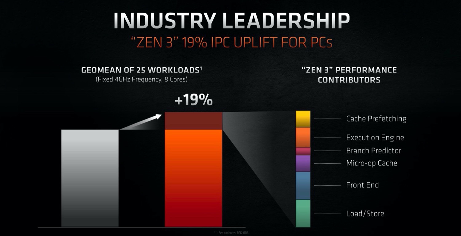
The AMD Ryzen 5 5600HS is a processor for big (gaming) laptops based on the Cezanne generation. The R5 5600H integrates six of the eight cores based on the Zen 3 microarchitecture. They are clocked at 3 GHz (guaranteed base clock) to 4.2 GHz (Turbo) and support SMT / Hyperthreading (12 threads). The chip is manufactured in the modern 7 nm process at TSMC. Compared to the 5600H (up to 52 W), the 5600HS is configured to a TDP of 35W.
The new Zen 3 microarchitecture offers a significantly higher IPC (instructions per clock) compared to Zen 2. For desktop processors AMD claims 19 percent on average and in applications reviews showed around 12% gains at the same clock speed.
With the increased clock speed and IPC improvements thanks to Zen 3, the Ryzen 5 5600H should be clearly faster than the lower clocked Ryzen 7 4600H.
In addition to the six CPU cores, the APU also integrates a Radeon RX Vega 6 integrated graphics card with 6 CUs and up to 1800 MHz. The dual channel memory controller supports DDR4-3200 and energy efficient LPDDR4-4266 RAM. Furthermore, 16 MB level 3 cache can be found on the chip.
The TDP of the APU is specified at 35 Watt and therefore also suited for thin gaming laptops.
AMD Ryzen 5 4680U
► remove from comparison
The AMD Ryzen 5 4680U is a semi-custom APU of the Renoir family designed for Microsoft devices. The 4680U integrates six CPU cores based on the Zen 2 microarchitecture clocked at 2.2 GHz (base) to 4 GHz (Boost) with SMT support for a total 12 threads. The two advantages a 4680U has over the older Ryzen 5 4600U are its higher base clock speed and a faster iGPU.
Architecture
The chip is manufactured on the modern 7 nm TSMC process and in part thanks to this fact, AMD advertises a 2x performance per watt improvement over the 12 nm Ryzen 3000 mobile processors. The built-in dual-channel memory controller supports LPDDR4-4266 RAM. Furthermore, 8 MB of L3 cache can be found on the chip.
Just like the other mobile Ryzen 4000 CPUs, a 4680U supports PCI-Express 3.0. Please go to our Renoir processor hub page for additional information on the product family.
Performance
Multi-thread performance is most comparable to the Ryzen 7 4700U and the Core i5-10500H, the latter being a much more power-hungry chip. This makes the Ryzen a more than decent CPU for most tasks, as of early 2022.
Graphics
In addition to the six CPU cores, the APU also integrates a DX 12 compatible Radeon RX Vega 7 graphics adapter with 7 CUs (448 unified shaders) at up to 1,500 MHz. The Vega iGPU will have no trouble HW-decoding AVC, HEVC and VP9 videos, but the newer AV1 codec will only be decoded via software. In terms of gaming, we are looking at an MX150-level performance. Pretty much all games released in 2020 can be played on low to medium settings in 720p on this graphics adapter.
Power consumption
This Ryzen 5 series chip has a default TDP (also known as the long-term power limit) of 15 W, a value that laptop makers - Microsoft, in this case - are free to change to anything between 10 W and 25 W, with clock speeds and performance changing accordingly as a result. Indeed, we saw the CPU consume roughly 23 watts when subjected to our usual stress testing routine.
The 7 nm TSMC process this Ryzen is built with makes for very decent, as of mid 2022, energy efficiency.
| Model | AMD Ryzen 5 5600HS | AMD Ryzen 5 4680U | ||||||||||||||||||||||||||||||||||||||||||||
| Series | AMD Cezanne (Zen 3, Ryzen 5000) | AMD Renoir (Ryzen 4000 APU) | ||||||||||||||||||||||||||||||||||||||||||||
| Codename | Cezanne-HS (Zen 3) | Renoir-U (Zen 2) | ||||||||||||||||||||||||||||||||||||||||||||
| Series: Renoir (Ryzen 4000 APU) Renoir-U (Zen 2) |
|
| ||||||||||||||||||||||||||||||||||||||||||||
| Clock | 3000 - 4200 MHz | 2200 - 4000 MHz | ||||||||||||||||||||||||||||||||||||||||||||
| L1 Cache | 384 KB | 384 KB | ||||||||||||||||||||||||||||||||||||||||||||
| L2 Cache | 3 MB | 3 MB | ||||||||||||||||||||||||||||||||||||||||||||
| L3 Cache | 16 MB | 8 MB | ||||||||||||||||||||||||||||||||||||||||||||
| Cores / Threads | 6 / 12 | 6 / 12 | ||||||||||||||||||||||||||||||||||||||||||||
| TDP | 35 Watt | 15 Watt | ||||||||||||||||||||||||||||||||||||||||||||
| Technology | 7 nm | 7 nm | ||||||||||||||||||||||||||||||||||||||||||||
| max. Temp. | 105 °C | 105 °C | ||||||||||||||||||||||||||||||||||||||||||||
| Socket | FP6 | FP6 | ||||||||||||||||||||||||||||||||||||||||||||
| Features | DDR4-3200/LPDDR4-4266 RAM, PCIe 3, MMX, SSE, SSE2, SSE3, SSSE3, SSE4A, SSE4.1, SSE4.2, AVX, AVX2, BMI2, ABM, FMA, ADX, SMEP, SMAP, SMT, CPB, AES-NI, RDRAND, RDSEED, SHA, SME | LPDDR4-4266 RAM, PCIe 3, MMX, SSE, SSE2, SSE3, SSSE3, SSE4A, SSE4.1, SSE4.2, AVX, AVX2, BMI2, ABM, FMA, ADX, SMEP, SMAP, SMT, CPB, AES-NI, RDRAND, RDSEED, SHA | ||||||||||||||||||||||||||||||||||||||||||||
| iGPU | AMD Radeon RX Vega 7 ( - 1800 MHz) | AMD Radeon RX Vega 7 ( - 1500 MHz) | ||||||||||||||||||||||||||||||||||||||||||||
| Architecture | x86 | x86 | ||||||||||||||||||||||||||||||||||||||||||||
| Announced | ||||||||||||||||||||||||||||||||||||||||||||||
| Manufacturer | www.amd.com | www.amd.com |
