Deutsch
 English
 Español
 Français
 Italiano
 Nederlands
 Polski
 Português
 Русский
 Türkçe
 Svenska
 Chinese
 Magyar
Apple M3 Pro 18-Core GPU vs AMD Radeon RX 7900M vs AMD Radeon RX 7700S
Apple M3 Pro 18-Core GPU
► remove from comparison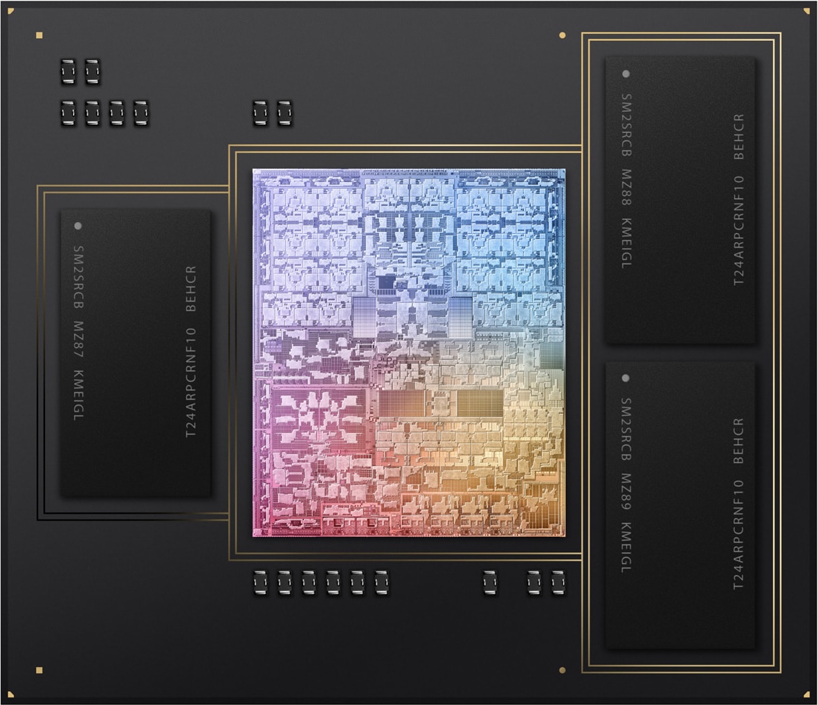
The Apple M3 Pro 18-Core GPU is a self-designed graphics card in the Apple M3 Pro (with 12 CPU cores) and offers all eighteen cores available on the chip. The graphics card uses a new architecture and now offers dynamic caching, mesh shading and ray tracing acceleration.
The GPU can access up to 36 GB LPDDR5-6400 unified memory via a 192-bit memory bus (max 150 GBit/s). Thanks to dynamic caching, the GPU only reserves as much memory as is required.
The entire chip is manufactured in the current 3nm process (probably N3B) at TSMC.
AMD Radeon RX 7900M
► remove from comparison
The AMD Radeon RX 7900M is a mobile upper high-end graphics card based on the Navi 31 chip (RDNA 3 architecture) manufactured in 5nm. It features 4,608 cores (72 CUs - compute units) and 16 GB of fast GDDR6 graphics memory connected with a 256 Bit memory bus. The chip also includes 64 MB Infinity Cache. The clock speed of the cores will depend on the laptop according to AMD. The specified game clock speed is 1825 MHz (most likely at 180 W TGP).
AMD compares the performance to the mobile RTX 4080 and shows a number of games where the 7900M is on average 7% faster. Raytracing is supported in hardware, but usually slower than the Nvidia counterpart. Nvidia also has the advantage of DLSS support in selected games.
The Navi 31 chip is manufactured at TSMC in the current 5nm process. The power consumption (TGP) is specified at 160 to 180 Watt (200 Watt including SmartShift from the CPU).
AMD Radeon RX 7700S
► remove from comparison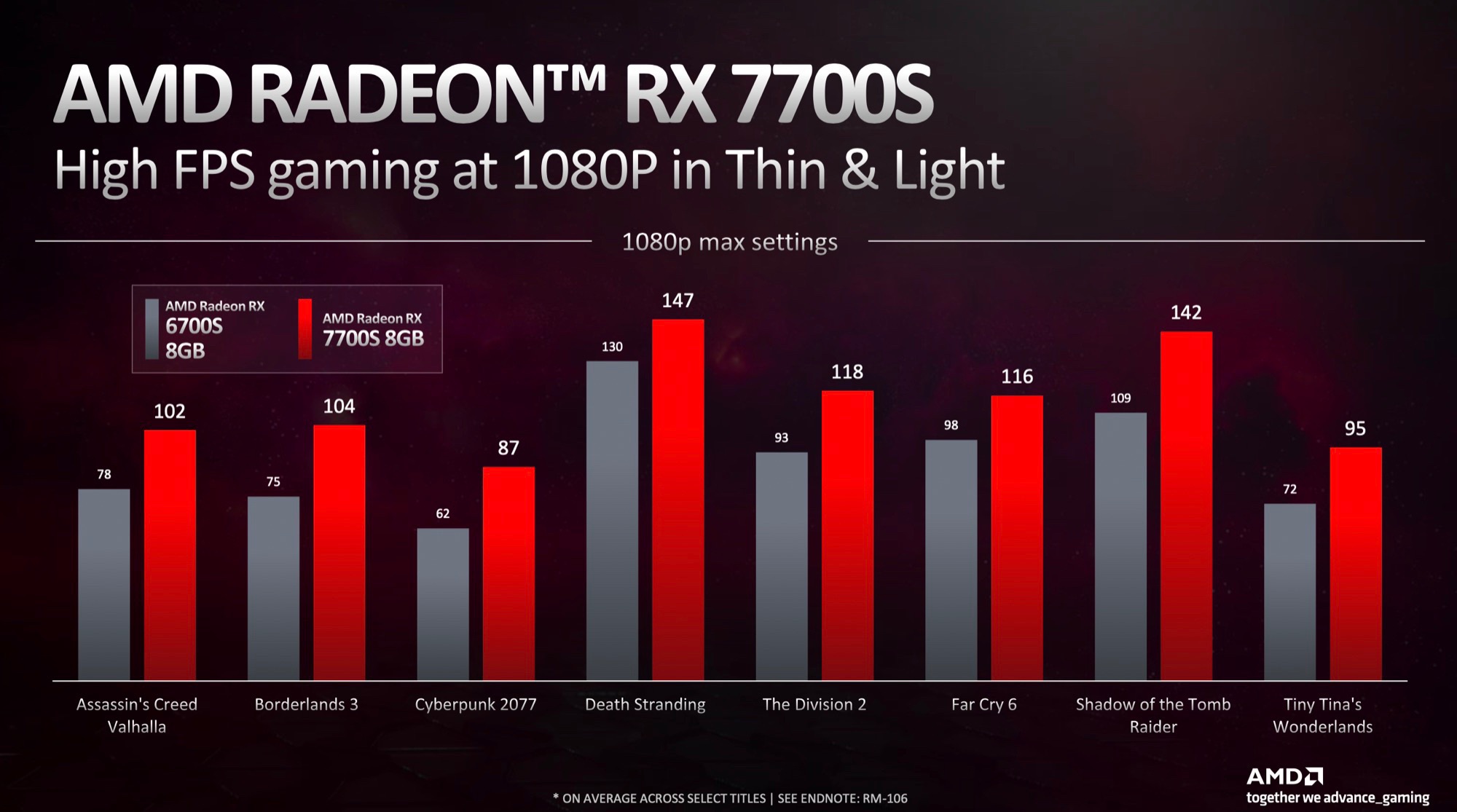
The AMD Radeon RX 7700S is a mobile upper mid-range graphics card based on the Navi 33 chip (RDNA 3 architecture) manufactured in 6nm. It features 2,048 cores (32 CUs - compute units) and 8 GB of fast GDDR6 graphics memory connected with a 128 Bit memory bus. The chip also includes 32 MB Infinity Cache. The clock speed of the cores will depend on the laptop according to AMD. The specified game clock speed is 2200 MHz (most likely at 100 W TGP). The 7700S is the power efficient version of the RX 7600M XT with slightly reduced clock speeds (-100 MHz) and TDP (-20W max).
AMD compares the performance to the old Radeon RX 6700S, that is easily beaten by the 7700S. As the theoretical performance is only slightly below the 7600M XT (at 100W TGP), the 7700S should also beat the RTX 3060 desktop GPU. Although the Raytracing performance did increase for RDNA 3, the GeForce GPUs are still faster in this regard.
The Navi 33 chip is manufactured at TSMC in the current 6nm process (versus 4nm of Nvidia RTX 4000 series). The power consumption (TGP) is specified at 75 to 100 Watt.
| Apple M3 Pro 18-Core GPU | AMD Radeon RX 7900M | AMD Radeon RX 7700S | |||||||||||||||||||||||||||||||||||||||||||||||||
| Radeon RX 7000M Series |
|
|
| ||||||||||||||||||||||||||||||||||||||||||||||||
| Pipelines | 18 - unified | 4608 - unified | 2048 - unified | ||||||||||||||||||||||||||||||||||||||||||||||||
| Memory Type | LPDDR5-6400 | GDDR6 | GDDR6 | ||||||||||||||||||||||||||||||||||||||||||||||||
| Shared Memory | no | no | no | ||||||||||||||||||||||||||||||||||||||||||||||||
| technology | 5 nm | 5 nm | 6 nm | ||||||||||||||||||||||||||||||||||||||||||||||||
| Notebook Size | medium sized | large | large | ||||||||||||||||||||||||||||||||||||||||||||||||
| Date of Announcement | 31.10.2023 | 19.10.2023 | 05.01.2023 | ||||||||||||||||||||||||||||||||||||||||||||||||
| Codename | Navi 31 | Navi 33 | |||||||||||||||||||||||||||||||||||||||||||||||||
| Architecture | RDNA 3 | RDNA 3 | |||||||||||||||||||||||||||||||||||||||||||||||||
| ROPs | 192 | 64 | |||||||||||||||||||||||||||||||||||||||||||||||||
| Core Speed | 1825 - 2090 (Boost) MHz | 2200 (Boost) MHz | |||||||||||||||||||||||||||||||||||||||||||||||||
| Theoretical Performance | 77.05 TFLOPS FP16, 38.52 TFLOPS FP32 | 31 TFLOPS FP16, 20.5 TFLOPS FP32 | |||||||||||||||||||||||||||||||||||||||||||||||||
| Cache | L3: 64 MB | L3: 32 MB | |||||||||||||||||||||||||||||||||||||||||||||||||
| Memory Speed | 18000 MHz | 18000 MHz | |||||||||||||||||||||||||||||||||||||||||||||||||
| Memory Bus Width | 256 Bit | 128 Bit | |||||||||||||||||||||||||||||||||||||||||||||||||
| Max. Amount of Memory | 16 GB | 8 GB | |||||||||||||||||||||||||||||||||||||||||||||||||
| Memory Bandwidth | 576 GB/s | 288 GB/s | |||||||||||||||||||||||||||||||||||||||||||||||||
| API | DirectX 12_2, Shader 6.7, OpenGL 4.6, OpenCL 2.2, Vulkan 1.3 | DirectX 12, Shader 6.4, OpenGL 4.6 | |||||||||||||||||||||||||||||||||||||||||||||||||
| Power Consumption | 180 Watt (160 - 200 Watt TGP) | 100 Watt (75 - 100 Watt TGP) | |||||||||||||||||||||||||||||||||||||||||||||||||
| Transistors | 53.9 Billion | 13.3 Billion | |||||||||||||||||||||||||||||||||||||||||||||||||
| Link to Manufacturer Page | www.amd.com | www.amd.com | |||||||||||||||||||||||||||||||||||||||||||||||||
| Die Size | 204 mm² |
| ||||||||||