 Deutsch
 English
 Español
 Français
 Italiano
 Nederlands
 Polski
 Português
 Русский
 Türkçe
 Svenska
 Chinese
 Magyar
Intel Core i7-6650U vs AMD A10-9600P
Intel Core i7-6650U
► remove from comparison
The Intel Core i7-6650U is an ULV (ultra low voltage) dual-core SoC based on the Skylake architecture. In September 2015, it's the fastest CPU of the 15 W series (besides the i7-6600U) and can be found in ultrabooks as well as normal notebooks. In addition to two CPU cores with Hyper-Threading clocked at 2.2 - 3.4 GHz (2 cores: max. 3.2 GHz), the chip also integrates an Iris Graphics 540 GPU with 64 MB of dedicated eDRAM memory and a dual-channel DDR4-2133/DDR3L-1600 memory controller. The SoC is manufactured using a 14 nm process with FinFET transistors.
Architecture
Skylake replaces both Haswell and Broadwell and brings the same microarchitecture in every TDP class from 4.5 to 45 W. The extensive improvements of the Skylake design include increased out-of-order buffers, optimized prefetching and branch prediction as well as additional performance gains through Hyper-Threading. Overall, however, performance per clock has been increased by only 5 to 10 percent (compared to Haswell) respectively under 5 percent (compard to Broadwell), which is quite modest for a new architecture ("Tock").
Furthermore, the organisation of the eDRAM cache has been modified. Instead of acting like a victim cache, which has to be adressed via the L3/LLC, the eDRAM can now be adressed directly by programms just like the main memory. The size is still 128 MB for the quad-core models (4C + GT4e), while the dual-core chips (2C + GT3e) only offer 64 MB.
Performance
According to the specified clock rates and the improved architecture, the Core i7-6650U should perform similar to a Core i5-4310M (Haswell, 37 W) and is one of the fastest ULV dual-cores as of late 2015. Thus, the CPU has sufficient power for office and multimedia purposes as well as more demanding applications and multitasking.
Graphics
The integrated graphics unit called Iris Graphics 540 represents the "GT3e" version of the Skylake GPU (Intel Gen. 9). The 48 Execution Units, also called EUs, are clocked at 300 - 1050 MHz and offer (thanks to the fast eDRAM cache) a performance sligthly above a dedicated GeForce 920M. Games of 2015 can thus be played smoothly in low or medium settings. For more information about performance and features, check our page for the Iris Graphics 540.
Power Consumption
Specified at a TDP of 15 W (including CPU, GPU and memory controller), the CPU is best suited for small notebooks and ultrabooks (11-inches and above). Optionally, the TDP can be lowered to 9.5 watts (cTDP down), reducing both heat dissipation and performance and allowing even more compact designs.
AMD A10-9600P
► remove from comparison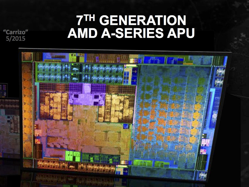
The AMD A10-9600P is a mid-range APU of the Bristol Ridge series (7th generation of APUs) with 4 CPU-cores (two Excavator modules) clocked at 2.4 - 3.3 GHz. It was announced in mid 2016 and is based on the same silicon as Carrizo but with more and refined features. It is a ULV-chip with a TDP of 15 Watt and integrates a Radeon R5 graphics card (384 shader cores / 6 compute cores) and a dual-channel DDR4-1866 memory controller. As Carrizo its a full featured SoC that offers all I/O ports on the chip.
The A10-9600P is slightly faster than the old 15-Watt top model of Carrizo, the FX-8800P. Therefore, the CPU performance is similar to a Broadwell 15 Watt Core i3 like The i3-5010U. See our Bristol Ridge article for more information on the architecture and improvements compared to Carrizo.
| Model | Intel Core i7-6650U | AMD A10-9600P | ||||||||||||||||||||||||||||||||||||||||||||||||||||||||||||||||||||||||||||||||||||
| Series | Intel Core i7 | AMD Bristol Ridge | ||||||||||||||||||||||||||||||||||||||||||||||||||||||||||||||||||||||||||||||||||||
| Codename | Skylake | Bristol Ridge | ||||||||||||||||||||||||||||||||||||||||||||||||||||||||||||||||||||||||||||||||||||
| Series: Bristol Ridge Bristol Ridge |
|
| ||||||||||||||||||||||||||||||||||||||||||||||||||||||||||||||||||||||||||||||||||||
| Clock | 2200 - 3400 MHz | 2400 - 3300 MHz | ||||||||||||||||||||||||||||||||||||||||||||||||||||||||||||||||||||||||||||||||||||
| L1 Cache | 128 KB | |||||||||||||||||||||||||||||||||||||||||||||||||||||||||||||||||||||||||||||||||||||
| L2 Cache | 512 KB | 2 MB | ||||||||||||||||||||||||||||||||||||||||||||||||||||||||||||||||||||||||||||||||||||
| L3 Cache | 4 MB | |||||||||||||||||||||||||||||||||||||||||||||||||||||||||||||||||||||||||||||||||||||
| Cores / Threads | 2 / 4 | 4 / 4 | ||||||||||||||||||||||||||||||||||||||||||||||||||||||||||||||||||||||||||||||||||||
| TDP | 15 Watt | 15 Watt | ||||||||||||||||||||||||||||||||||||||||||||||||||||||||||||||||||||||||||||||||||||
| Technology | 14 nm | 28 nm | ||||||||||||||||||||||||||||||||||||||||||||||||||||||||||||||||||||||||||||||||||||
| max. Temp. | 100 °C | 90 °C | ||||||||||||||||||||||||||||||||||||||||||||||||||||||||||||||||||||||||||||||||||||
| Socket | BGA | |||||||||||||||||||||||||||||||||||||||||||||||||||||||||||||||||||||||||||||||||||||
| Features | Dual-Channel DDR3L-1600/DDR4-2133 Memory Controller, HyperThreading, AVX, AVX2, Quick Sync, Virtualization, AES-NI, vPro, TXT | Dual-Channel DDR3/DDR4-1866 Memory Controller, PCIe 3.0 x8 | ||||||||||||||||||||||||||||||||||||||||||||||||||||||||||||||||||||||||||||||||||||
| iGPU | Intel Iris Graphics 540 (300 - 1050 MHz) | AMD Radeon R5 (Bristol Ridge) ( - 720 MHz) | ||||||||||||||||||||||||||||||||||||||||||||||||||||||||||||||||||||||||||||||||||||
| Architecture | x86 | x86 | ||||||||||||||||||||||||||||||||||||||||||||||||||||||||||||||||||||||||||||||||||||
| $415 U.S. | ||||||||||||||||||||||||||||||||||||||||||||||||||||||||||||||||||||||||||||||||||||||
| Announced | ||||||||||||||||||||||||||||||||||||||||||||||||||||||||||||||||||||||||||||||||||||||
| Manufacturer | ark.intel.com | products.amd.com | ||||||||||||||||||||||||||||||||||||||||||||||||||||||||||||||||||||||||||||||||||||
| Transistors | 3100 Million | |||||||||||||||||||||||||||||||||||||||||||||||||||||||||||||||||||||||||||||||||||||
| Die Size | 250 mm2 |
